


P R E L I M I N A R Y
AMD
43Am79C930
PCMCIA Interface —
The Am79C930 device fully sup-
ports the PCMCIA standard, revision 2.1.
The PCMCIA interface on the Am79C930 device sup-
ports both memory and I/O cycles. The data bus is 8 bits
in width. The address bus is 15 bits in width. Memory ac-
cesses are enabled by default at power up. I/O ac-
cesses are enabled only when the ConfIndex bits of the
PCMCIA Configuration Option Register have a
non-zero value. It is not possible to disable the memory
access response function. The Am79C930 device re-
quires 32K of Common memory space and 16 or 40
bytes of I/O space. Since all Am79C930-based memory
resources are also mapped into an I/O port, it is
possible to operate with a Common memory space allo-
cation of 0 bytes.
The Am79C930 device supports the Card Information
Structure and the Card Configuration Registers defined
in the PCMCIA 2.1 standard, by decoding 2K+4 bytes of
Attribute memory space. The first tuple of the Card Infor-
mation Structure must be located at PCMCIA Attribute
Memory location 0h. Note that in the Am79C930 device,
Attribute Memory locations 000h–07FFh are mapped to
the upper 1 Kbytes of the 128K Flash memory space
(i.e., Flash memory locations 1FC00h–1FFFFh). The
upper 1K–16 byte locations of the Flash memory device
must be reserved for PCMCIA Card Information Struc-
ture use. (The uppermost 16 bytes of the Flash memory
may not be used for PCMCIA CIS space, since the
80188 core will fetch its first instructions from these lo-
cations following a reset operation. These locations cor-
respond to PCMCIA Attribute memory
locations 7F0h–7FFh.)
Note that the 2 Kbytes of Attribute memory
0000h–07FFh are mapped to only 1 Kbytes of Flash
memory. Since the PCMCIA specification indicates that
only even addressed bytes of Attribute memory are de-
fined to exist, only the even addressed 1K of the 2K At-
tribute memory space is actually physically present.
Odd addressed Attribute memory locations in the
Am79C930 device are undefined.
While the Common memory space of the Am79C930
device only accommodates access to 32 Kbytes of
Common memory, the Am79C930 device uses device
select and bank select bits (bits 5:3 of the BSS
register (SIR1)) in order to access a total of 256K of
memory space.
When accessing Common memory resources through
PCMCIA common memory accesses, lower memory
addresses at the PCMCIA interface are passed directly
to the memory interface bus, and the Flash Memory
Chip Enable (FCE) or the SRAM Chip Enable (SCE) sig-
nal is asserted, depending upon the value of SIR1[5].
The upper two bits of the memory interface address bus
are set according to the value of SIR1[4:3]. The
PCMCIA memory access control signals (WE, OE,
CE1) are automatically translated into the appropriate
memory interface signals (RD, WR).
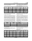
The PCMCIA Card Configuration registers that are sup-
ported are the Configuration Option Register and the
Card Configuration and Status Register. These two reg-
isters are physically located in the Bus Interface Unit
and logically exist
only
in PCMCIA Attribute memory
space (i.e., they are not also mapped to Common
memory space.) They are located at Attribute memory
locations 0800h and 0802h, respectively. The location
of these registers is fixed. Therefore, the information
programmed into the CIS
must
give the value 2K
(=0800h) as the Card Configuration Registers Base
Address in the TPCC_RADR field of the
Configuration Tuple.
The PCMCIA Card Configuration registers are the only
writable PCMCIA Attribute memory locations within the
Am79C930, because these two registers do
not
corre-
spond to Flash memory locations, and these two loca-
tions are not CIS structures.
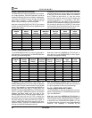
The Am79C930 device occupies either 16 bytes of I/O
space or 40 bytes of I/O space, depending upon the set-
ting of the EIOW bit (bit 2 of the BSS register (SIR1)).
The I/O space of the Am79C930 contains the General
Configuration Register, the Bank Switching Select
Register, and the set of 32 TIR registers. Additionally, all
Am79C930 resources are accessible through I/O ac-
cesses (i.e., all
memory
structures are accessible
through the Local Memory Address and I/O Data Ports).
The Local Memory Address port (SIR2,3) plus SIR1[5:3]
function together as a pointer to the memory resources
of the Am79C930 device. SIR1[5] determines the de-
vice selected (SRAM or Flash) and SIR1[4:3] and
LMA[14:0] supply the address to the selected device
whenever the I/O Data Port is read or written. Whenever
any of the four I/O Data Ports is accessed, then the Lo-
cal Memory Address Port value is automatically incre-
mented by a value of 1.
Because of the existence of the Local Memory Address
and I/O Data Ports, the Am79C930 device may be
used in an I/O only fashion. Appropriate configuration
information may be placed into the CIS space so that the
PCMCIA configuration utility will assign no memory
space to the Am79C930-based design. Note, however,
that the Am79C930 device will always respond to Com-
mon memory accesses that are directed to the
0000h–7FFFh range, if they occur in the PCMCIA slot in
which the Am79C930-based design resides. The
Common memory slave response function is always ac-
tive on the Am79C930 device; it is not possible to dis-
able this function. The Am79C930 device does not
attempt to interpret the ConfIndex value of the PCMCIA
Configuration Option Register except for purposes of
enabling the I/O slave response function.