


P R E L I M I N A R Y
AMD
137Am79C930
AC CHARACTERISTICS
5.0 V MEMORY BUS INTERFACE
ABSOLUTE MAXIMUM RATINGS
Storage Temperature: –65 to +150°C. . . . . . . . . . . .
Ambient Temperature Under Bias: –65 to +125°C. . .
Supply Voltage to AVSS
or DVSS (AVDD, DVDD): –0.3 to +6 V. . . . . . . . . . . . . .
Stresses above those listed under Absolute Maximum
Ratings may cause permanent device failure. Functionality at
or above these limits is not implied. Exposure to Absolute
Maximum Ratings for extended periods may affect
device reliability.
OPERATING RANGES
Commercial (C) Devices
Temperature (T
A)0°C to + 70°C. . . . . . . . . . . . . . . . .
Supply Voltages (V
CC, VDDT, VDDU1, VDDU2, VDDM, VDDP)
4.75 V to 5.25 V. . . . . . . . . . . . . . . . . . . . . . . . . . . . .
Supply Voltages
(AV
DD, VDD5) +5 V ± 5%. . . . . . . . . . . . . . . . . . . . . . . .
All inputs within the range: V
SS – 0.5 V ≤ VIN ≤ VDD + 0.1 X
V
DD – where VSS and VDD are appropriate reference pins
for a given input pin. (See section on power supply
pin descriptions.)
CL = 50 pF unless otherwise noted
Operating ranges define those limits between which the func-
tionality of the device is guaranteed.
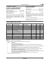
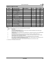
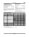
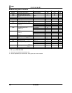
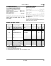
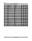
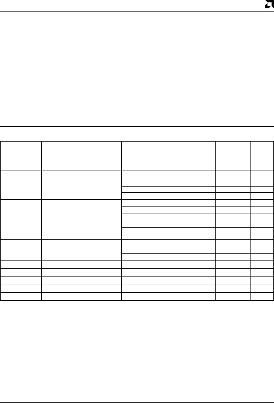
MEMORY BUS READ ACCESS
Parameter
Symbol Parameter Description Test Conditions Min Max Unit
tmAD MA[16:0] valid from CLKIN ↓ 260ns
tmCD CE active delay from CLKIN ↓ Note 1 2 60 ns
tmOD MOE active delay from CLKIN ↓ 260ns
tmOLZ MOE ↓ to MD[7:0] driven 0 wait states 0 30 ns
(Note 3) 1 wait state 80 ns
2 wait states 130 ns
tmAA Address Read Access Time 0 wait states 55 ns
(Note 3) 1 wait state 105 ns
2 wait states 155 ns
tmACS CE Read Access Time 0 wait states 55 ns
(Notes 1, 3) 1 wait state 105 ns
2 wait states 155 ns
tmOE MOE Read Access Time 0 wait states 30 ns
(Note 3) 1 wait state 80 ns
2 wait states 130 ns
tmRI CE Inactive Time Notes 1, 2 0 ns
tmAH MA[16:0] valid hold from MOE ↑ Note 1 TCLKIN-10 ns
tmCH CE valid hold from MOE ↑ TCLKIN-10 ns
tmH MD[7:0] valid hold from MOE ↑ Note 2 0 ns
tmHZ MD[7:0] inactive from MOE ↑ Note 2 0 2 X TCLKIN-15 ns
Notes:
1.
CE
= one of:
FCE
,
SCE
,
XCE
2. Parameter not included in the production test.
3. Value is dependent upon TCLKIN value. Value given is for CLKIN = 40 MHz.