


P R E L I M I N A R Y
AMD
71Am79C930
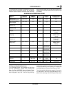
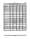
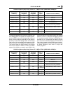
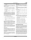
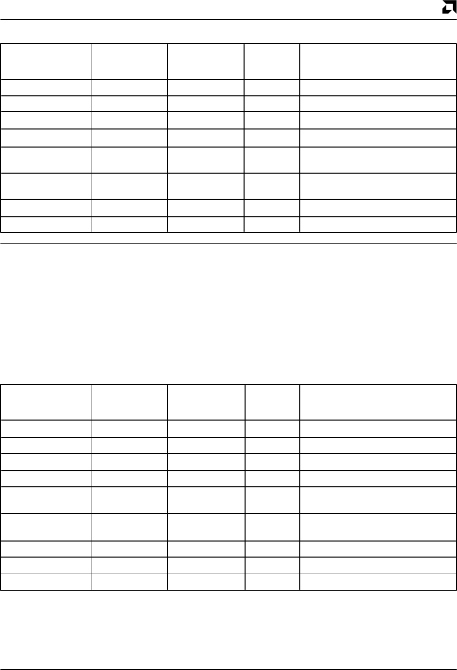
80188 Core Memory Map Using Scheme “A”, LMCS=1FF8h, UMCS=E038h, MIR0[6]=0
Active
80188 Address Active 80188 Am79C930 Size of
in Memory Chip Select Chip Select Space Physical Location of Memory
0 0000h–0 03FFh LCS SCE 1 Kbytes SRAM Memory 0 0000h–0 03FFh
0 0400h–0 041Fh LCS none 32 bytes TIR 0–31
0 0420h–0 042Fh LCS none 16 bytes MIR 0–15
0 0430h–0 043Fh LCS XCE 16 bytes XCE locations 0–15
0 0440h–0 047Fh LCS none 64 bytes Reserved for future use–access to
these areas is currently undefined
0 0480h–1 FFFFh LCS SCE 128K– SRAM Memory 0 0480h–1 FFFFh
1K–128 bytes
2 0000h–D FFFFh none none 768 Kbytes Undefined
E 0000h–F FFFFh UCS FCE 128 Kbytes Flash Memory 0 0000h–1 FFFFh
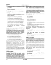
The second mapping scheme (scheme “B”) places 32K
of the SRAM, the 32 TIR registers, the 16 MIR registers,
and the 16 XCE locations into the lowest 32K of memory
space, and then maps the upper 96K of Flash memory
to memory locations 32K through 128K. All 128K of the
Flash memory is also available at the uppermost 128K
memory locations of the 80188 core’s address space.
This scheme allows the LMCS register of the 80188
core be set to 07F8h or 0FF8h or 1FF8h. The UMCS
register of the 80188 core must be set to E038h. Also
required is that bit 6 of the MIR0 register (the mapping
select bit) is set to 1. Note that with mapping scheme
“B”, a maximum of 32K–128 bytes of SRAM space is
available for use. The advantage of mapping scheme
“B” is that when all 80188 firmware can fit into 32K of
Flash memory space and the SRAM memory require-
ment for the application is less than or equal to 32K, then
all 80188 operations occur within a single 64K
memory segment.
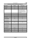
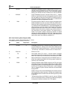
80188 Core Memory Map Using Scheme “B”, LMCS=1FF8h, UMCS=E038h, MIR0[6]=1
Active
80188 Address Active 80188 Am79C930 Size of
in Memory Chip Select Chip Select Space Physical Location of Memory
0 0000h–0 03FFh LCS SCE 1 Kbytes SRAM Memory 0 0000h–0 03FFh
0 0400h–0 041Fh LCS none 32 bytes TIR 0–31
0 0420h–0 042Fh LCS none 16 bytes MIR 0–15
0 0430h–0 043Fh LCS XCE 16 bytes XCE locations 0–15
0 0440h–0 047Fh LCS none 64 bytes Reserved for future use–access to
these areas is currently undefined
0 0480h–0 7FFFh LCS SCE 32K– SRAM Memory 0 0480h–1 FFFFh
1K–128 bytes
0 8000h–1 FFFFh don’t care FCE 96 Kbytes Flash Memory 0 8000h–1 FFFFh
2 0000h–D FFFFh none none 768 Kbytes Undefined
E 0000h–F FFFFh UCS FCE 96 Kbytes Flash Memory 0 0000h–1 FFFFh