


P R E L I M I N A R Y
AMD
83Am79C930
MIR8: Flash Wait States
This register gives the Flash Wait states.
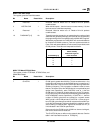
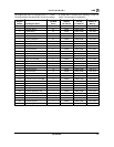
Bit Name Reset Value Description
7:4 Reserved – Reserved. Must be written as a 0. Reads of this bit produce
undefined data.
3 HOSTALLOW 1 When this bit equals 1, then the host can access memory; if 0, then
the host access is blocked completely
2 Reserved – Reserved. Must be written as a 0. Reads of this bit produce
undefined data.
1:0 FLASHWAIT[1:0] 11b These bits must be set equal to or greater than the number of wait
states that are generated internally in the 80188 core as defined by
the programming of the R1 and R0 bits of the 80188 UMCS register.
Wait states programmed into FLASHWAIT will cause wait states to
be inserted into 80188 access to Flash and system accesses to
Flash. Each wait state added to a Flash access is equivalent to two
CLKIN periods. These bits are interpreted as follows:
Number Of Wait
States Used By
Arbitration Logic For
FLASHWAIT[1:0] Flash Accesses
11 3
10 2
01 1
00 0
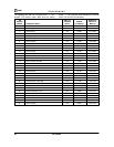
MIR9: TCR Mask STSCHG Data
This register contains TCR Mask, STSCHG Data, and
SRAM Wait States.
Bit Name Reset Value Description
7 CLKGT20 1 CLKIN input is greater than 20 MHz. This bit must be set to a 1 by
the 80188 code whenever the Am79C930 device is operating in a
system that uses a source for the CLKIN input that is greater than
20 MHz in frequency. This information is needed in order to insure
that the TAI section of the Am79C930 device is not pushed beyond
design limits. Specifically, when CLKGT20 is set to 1, then the
CLKIN signal is divided by 2 before being fed to the TAI section.
CLKGT20 is also used to calibrate the time delay generated by the
HOSTLONGWAIT counter. Specifically, if CLKGT20 = 1, then the
number of CLKIN cycles that are counted for a system access
WAIT period is 192 CLKIN periods; if CLKGT20 = 0, then the num-
ber of CLKIN cycles that are counted for a system access WAIT pe-
riod is 96 CLKIN periods. This time adjustment is needed in order to
avoid creating a PCMCIA WAIT signal that exceeds the 12.1 µs
limit indicated in the PCMCIA specification.
If the source for the CLKIN input is a 20 MHz or slower clock signal,
then this bit should remain reset at 0.
The CLKGT20 bit has an effect on the network data rate. See the
table in the Data Rate bit section in TCR30[2:0].