AMD
P R E L I M I N A R Y
32
Am79C930
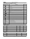
IEEE 1149.1 Test Access Port Pins
TCK
Test Clock
Input
TCK is the clock input for the boundary scan test mode
operation. TCK frequency may be as high as 10 MHz.
TCK does not have an internal pull-up resistor and must
be connected to a valid TTL or CMOS level at all times.
TCK must not be left unconnected.
TDI
Test Data Input
Input
TDI is the test data input path to the Am79C930 device.
If left unconnected, this pin has a default value of HIGH.
TDO
Test Data Output
Output
TDO is the test data output path from the Am79C930 de-
vice. TDO is tri-stated when the JTAG port is inactive.
TMS
Test Mode Select
Input
TMS is a serial input bit stream is used to define the spe-
cific boundary scan test to be executed. If left uncon-
nected, this pin has a default value of HIGH.
TRST
Test Reset
Input
When asserted, TRST will asynchronously reset the
IEEE 1149.1 state. The reset state of the IEEE 1149.1
state machine is FFh.
Test Pin
TEST
Test
Input
The TEST pin should be tied HIGH and is reserved for
internal factory test only.
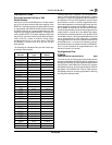
Power Supply Pins
Analog Power Supply Pins
AVDD
Analog Power (1 Pin)
Power
There is one analog 5 V supply pin. This supply pin pro-
vides power to the analog section of the Am79C930 de-
vice. This pin must always be connected to 5 V, unless
the A/D function of the device is not required. If the A/D
function of the device is not required, then this pin may
be connected to either a 5 V supply or to a 3.3 V supply.
Note: A/D must be disabled.
However, all analog power
pins (AVDD and VDD5) must be connected to the same
supply voltage. Special attention should be paid to the
printed circuit board layout to avoid excessive noise on
the AVDD line.
AVSS
Analog Ground (1 Pin)
Ground
There is one analog ground pin. This ground pin pro-
vides ground reference to the analog section of the
Am79C930 device. This pin must always be connected
to a ground supply. Special attention should be paid to
the printed circuit board layout to avoid excessive noise
on the AVSS line.
VDD5
A/D Power (1 Pins)
Power
There is one A/D power supply pin. This pin provides
power to the A to D converter circuit. This pin must
always be connected to a 5 V supply unless the A/D
function of the device is not required. If the A/D function
of the device is not required, then this pin may be con-
nected to either a 5 V supply or to a 3.3 V supply. How-
ever, all analog power pins (AVDD and VDD5) must be
connected to the same supply voltage. Special attention
should be paid to the printed circuit board layout to avoid
excessive noise on the VDD5 line.
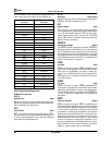
Digital Power Supply Pins
VDDT
Transceiver Power (2 Pins)
Power
There are two transceiver interface power supply pins.
These pins provide power to the transceiver interface
buffers and drivers on pins 98 through 133. These pins
may be connected to either a 5.0 V supply or a 3.3 V sup-
ply, but both of these pins must be connected to the
same supply voltage.
VSST
Transceiver Ground (4 Pins)
Ground
There are four transceiver interface ground pins. These
pins provide ground reference to the transceiver
interface buffers and drivers on pins 98 through 133. In
both 5 V and 3 V systems, these pins should be con-
nected to a ground supply.
VCC
Core Logic Power (2 Pins)
Power
There are two core logic power supply pins. These pins
provide power to the core logic and must always be
less than or equal to VDDT, VDDU1, VDDU2, VDDP,
and VDDM.


