


AMD
P R E L I M I N A R Y
84
Am79C930
6 Reserved – Reserved. Must be written as a 0. Reads of this bit produce
undefined data.
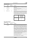
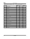
5:4 SRAMWAIT[1:0] 11b These bits must be set equal to or greater than the number of wait
states that are generated internally in the 80188 core as defined by
the programming of the R1 and R0 bits of the 80188 LMCS register.
Wait states programmed into SRAMWAIT will cause wait states to
be inserted into 80188 access to SRAM and system accesses to
SRAM. Each wait state added to an SRAM access is equivalent to
two CLKIN periods. These bits are interpreted as follows.
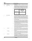
Number Of Wait
States Used By
Arbitration Logic For
SRAMWAIT[1:0] SRAM
11 3
10 2
01 1
00 0
3 HOSTLONGWAIT 0 When HOSTLONGWAIT is set to a 1, 96, or 192 CLKIN periods
(depending upon the setting of the CLKGT20 bit of MIR9) of
READY DELAY are added to all system access cycles that are di-
rected to Flash, SRAM and TAI registers. (Note that accesses to
PCMCIA registers, SIR registers and ISA PnP register are unaf-
fected.) This delay is nominally 4.8 µs when CLKIN = 20 MHz and
CLKGT20 is set to 0, and nominally 4.8 µs when CLKIN = 40 MHz
and CLKGT20 is set to 1.
When HOSTLONGWAIT is set to a 0, all host (system) access cy-
cles will be delayed according to their position in the arbitration
queue, where the only other master competing is the 80188 core
and the requesting device has priority over the current master (i.e.,
worst case READY delay with HOSTLONGWAIT set to 0 is equal to
1 access performed by other master plus the number of wait states
for the device being accessed.)
System write accesses will be posted and, therefore, may not im-
mediately experience the “longwait” delay. However, the posted ac-
cess must internally wait for the “longwait“ before becoming
completed and this will cause a subsequent system access to expe-
rience the full 4.8 µs wait time plus an additional 4.8 µs wait time for
a total of 9.6 µs. Note, however, that the average wait time per host
cycle in this case will still be 4.8 µs.
2 INITDN 0 Initialization Done. When set to a 0, this bit enables the pull up and
pull down devices that are attached to the various multi-function
pins. When set to a 1, the pull up and pull down devices are
disabled, reducing standby current consumption to the minimum
possible level.
1 TCR Mask 0 TCR Mask. When set to a 1, writes to TCR13, TCR14, and TCR15
are ignored. This bit is provided as a security measure against acci-
dental reprogramming of network interface pin function by poorly
directed system accesses which could cause output-to-output con-
nections to become established.
0 STSCHGD 0 STSCHG Data. If the STSCHGFN bit of TCR15 has been set to a 1,
and the WAKEUP bit of the PCMCIA CCSR is set to a 1, then this bit
may be written with a 1 and writing a 0 to this bit has no effect. If the
STSCHGFN bit of TCR15 has been set to a 1, then STSCHGD is
reset to a 0 automatically whenever the WAKEUP bit of the