


P R E L I M I N A R Y
AMD
91Am79C930
The value read from SDD will always represent the current value of
the SDDATA pin. The complete control of the function of the
SDDATA pin is described in the
Multi-Function Pin
section.
When the fast serial port (TIR3) is used, then the value written to
SDD will be exclusive OR’d (XOR) with the data from the FSD bits
of TIR3 before the FSD bits are sent to the SDDATA pin.
TIR3: Fast Serial Port Control
This register provides a relatively quick write access to
the Serial Port signals of the device (i.e., SDCLK and
SDDATA). The SDSEL3-1 signals must be previously
set with an access to the Serial Port control register
(TIR2). The SDDT bit of TIR2 must be set to 0 or the fast
write will fail. A write to the TIR3 register will initiate the
fast serial transfer. A read from this register will not
cause any activity at the serial port pins. The clock for
the serial port write operation will be created from the
CLKIN signal when the CLKGT20 bit of MIR9 is set to 0
and from the CLKIN signal divided by two when the
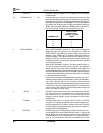
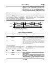
CLKGT20 bit of MIR9 is set to 1. Timing for the fast read
operation is as follows:
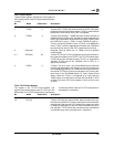
20138B-8
SDDATA
SDCLK
tA
tA = period of CLKIN when CLKGT20 = 0
tA = (period of CLKIN) X 2 when CLKGT20 = 1
2 X tA
tA tA
2 X tA
tA tA
2 X tA
tA
Figure 3. Serial Port Fast Read Timing
Bit Name Reset Value Description
7:5 BCNT[2:0] – Byte Count. From 1 to 5 bits of the FSD[4:0] data may be sent dur-
ing one fast access to the serial port. The value of BCNT[2:0] deter-
mines exactly how many bits will be sent for any access. The value
BCNT[2:0] = 1 represents a value of one bit to be sent.
4:0 FSD[4:0] – Fast Serial Data[4:0] This is the data that is sent out during the Fast
Serial port access. Bit 0 is sent first. FSD bit values are exclusive
OR’d (XOR) with the value written to the SDD bit of TIR2[0] before
being sent to the SDDATA pin.
TIR4: Interrupt Register 1
The TAI Interrupt Register 1 provides interrupt status in-
formation. Any interrupt bit may be cleared by writing a 1
to the bit location. Writing a 0 to a bit location has no ef-
fect on the bit value. When the unmask bit for any
interrupt is set to 0, then the bit in the Interrupt register
may still become set, but no interrupt to the 80188 em-
bedded controller will occur.
Bit Name Reset Value Description
7 CHBSYC 0 CHBSY Change of state. Indicates that there is a change of state in
the CCA indication.
6 ANTSW 0 Antenna Switch. This bit will become set at the end of each time slot
as programmed in the Antenna Diversity Timer Register (TCR4) to
indicate that the channel tests for this antenna selection have been
completed. This bit is reset to 0 when the RXRES bit of TIR16 is set
to 1, or if a 1 is written to ANTSW.