


P R E L I M I N A R Y
AMD
45Am79C930
Memory Interface
The memory interface is provided to support direct con-
nection of both a non-volatile memory (typically Flash
memory) and an SRAM and an additional peripheral de-
vice. Separate chip enables for Flash, SRAM, and an
extra peripheral device exist in the memory interface.
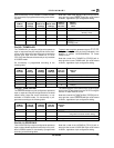
The 32K range of address space visible at the system
interface (either PCMCIA or ISA Plug and Play) maps to
a total of 256K of memory through the use of a device
select bit and bank switching bits in the Bank Switching
Select register (SIR1). 128K of space is reserved
for Flash memory and 128K of space is reserved for
SRAM. The 32 bytes of space reserved for the extra pe-
ripheral device are only accessible by the embedded
80188 core.
The internal Transceiver Attachment Unit also resides
on the memory interface bus and uses 8 bytes (or 32)
bytes of I/O space as viewed by the system interface.
These same registers occupy 32 bytes of the SRAM’s
memory space (i.e., instead of I/O space) as viewed by
the embedded 80188 core. The MIR registers of the BIU
occupy an additional 16 bytes of SRAM space as
viewed by the embedded 80188 core. The MIR registers
are not visible to the system interface.
The memory interface bus is shared between the sys-
tem interface and the embedded 80188 processor.
Memory interface bus sharing between the system in-
terface and the 80188 processor core is based upon an
equal priority delivered in a round robin fashion. When-
ever the system interface is accessing a device on the
memory interface bus, then the 80188 core is placed
into ready wait. Whenever the 80188 core is accessing a
device on the memory interface bus, then the system in-
terface bus activity will be given a ready wait. When the
current memory interface bus master has completed its
cycle, then the other memory interface bus master will
be given control of the memory interface bus.
The 80188 memory accesses are directed toward
Flash, SRAM, the XCE peripheral device, TAI registers
(TIR/TCR), or BIU registers (MIR) according to the UCS
and LCS signals of the 80188 core. Normally, whenever
UCS is active during an 80188 memory access, the ac-
cess is directed toward the Flash memory; and when-
ever LCS is active during an 80188 memory access, the
access is directed toward the SRAM memory or the
XCE peripheral device or the TAI registers or BIU regis-
ters. Along with the UCS and LCS signals, 17 of the
80188 address lines are internally connected through
the BIU to the memory interface bus, allowing 256K of
memory to be addressed by the 80188. (128K of Flash
and 128K of SRAM/XCE/TAI/BIU may be addressed by
the 80188, for a total of 256K of memory.)
An alternate addressing mode will alias the upper
96 Kbytes of Flash memory into the upper 96 Kbytes of
SRAM space, while preserving the location of the lower
32K of SRAM, the XCE peripheral, and the TAI/BIU
registers. This mode allows for 32K of SRAM/XCE/TAI/
BIU and 32K of Flash to reside in a single 64 Kbyte seg-
ment of 80188 memory space. This mode is selected
through a bit in the MIR0 register.
The TAI connects to only a portion of the memory inter-
face bus. Specifically, the lowest five address bits and
the entire data bus of the memory interface connect to
the TAI. A separate internal chip select signal for the TAI
exists to avoid confusion among slave devices. This sig-
nal is not available on the Am79C930 memory interface
bus, and therefore, memory interface cycles may be ob-
served for which neither the Flash chip enable, nor the
SRAM chip enable, nor the XCE signal is asserted.
Similar behavior is observed when the 80188 core is ac-
cessing registers which are located within the BIU.
Embedded 80188
The embedded 80188 core provides the basic means
for implementing IEEE 802.11 (draft) MAC functionality.
The elements of the Am79C930 device that are involved
in MAC function include the 80188 core, the Flash mem-
ory, the SRAM memory, the timers within the 80188, the
sleep timer in the BIU, the Transceiver Attachment Unit,
and the associated busses and signaling that connect
the 80188 core to the BIU and the Transceiver
Attachment Unit.
The Am79C930 device directly incorporates some of
the basic protocol requirements for operation of a IEEE
802.11 (draft) node. Other portions of the IEEE 802.11
(draft) MAC protocol need to be created with appropri-
ate firmware written to execute on the 80188 core.
With proper 80188 coding, the Am79C930 device
can be made to operate according to the
IEEE 802.11 (draft).
Media Access Management
— The IEEE 802.11
(draft) protocol defines a media access mechanism
which permits all stations to access the channel with
equality. Synchronous time-bounded service and asyn-
chronous time-bounded access service are also defined
in the IEEE 802.11 (draft) specification. Any node can
attempt to contend for the channel by waiting for a pre-
determined time (Inter Frame Spacing) after the last ac-
tivity, and then waiting an additional random backoff
time before determining whether to attempt to transmit
on the media. If two or more nodes simultaneously con-
tend for the channel, their signals will interact causing
loss of data, defined as a collision. It is the responsibility
of the MAC to attempt to avoid and recover from a colli-
sion in order to insure data integrity for the end-to-end
transmission to the receiving station.
Medium Allocation
The IEEE 802.11 (draft) standard requires that each
Carrier Sense Multiple Access/Collision Avoidance
(CSMA/CA) MAC monitor the medium for traffic by
watching for carrier activity. When carrier is detected,