


AMD
P R E L I M I N A R Y
132
Am79C930
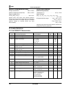
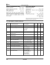
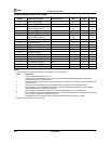
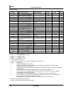
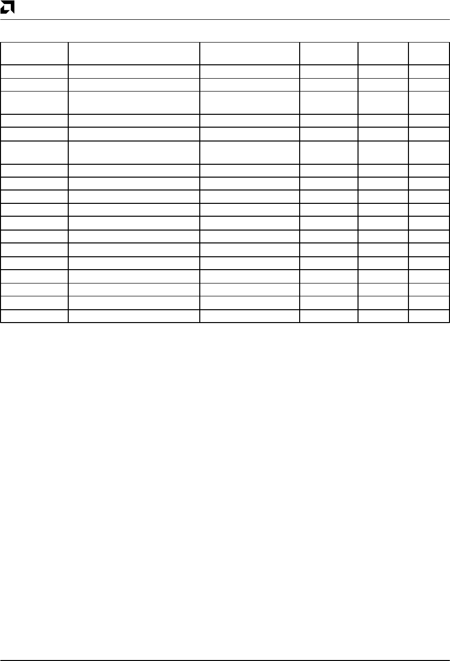
PCMCIA MEMORY WRITE ACCESS
Parameter
Symbol Parameter Description Test Conditions Min Max Unit
tAVWL Address setup to WE ↓ 20 ns
tAVWH Address setup to WE ↑ 100 ns
tWMAX Write recovery time
(Address hold from WE ↑ )20ns
tELWH CE setup to WE ↑ 140 ns
tELWL CE setup to WE ↓ 0ns
tGHEH CE hold from OE ↑ (READ) or CE
hold from WE ↑ (WRITE) 20 ns
tGHWL OE setup to WE ↓ 10 ns
tWHGL OE hold from WE ↑ 10 ns
tWLWH WE pulse width 120 ns
tWLWTV WAIT valid from WE ↓ 35 ns
tWTLWTH WAIT pulse width Notes 1, 2 53 X TCLKIN ns
tWTHWH WE hold from WAIT ↑ 0ns
tDVWH Data setup to WE ↑ 60 ns
tWMDX Data hold from WE ↑ 30 ns
tGHQZ Data disabled from OE ↑ Note 2 90 ns
tWLQZ Data disabled from WE ↓ Note 2 90 ns
tWHQNZ Data enabled from WE ↑ Note 2 5 ns
tGLQNZ Data enabled from OE ↓ Note 2 5 ns
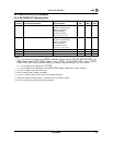
Notes:
1. The max value for this parameter assumes the following worst case situation:
Value Worst Case
0 FLASH and SRAM wait states set at “3.”
1 Host performs PCMCIA WRITE cycle at same time that Am79C930 embedded 80188 controller begins
instruction fetch cycle to FLASH memory.
2 PCMCIA WRITE cycle is posted internal to Am79C930 device, pending the completion of the embedded 80188
controller access.
3 Host performs PCMCIA READ cycle immediately following completion of PCMCIA WRITE cycle.
4 After completion of first embedded 80188 access to FLASH, posted PCMCIA WRITE executes to SRAM;
PCMCIA READ stycle is being held in wait state.
5 After completion of posted ISA WRITE cycle, new embedded 80188 access to FLASH begins.
6 After completion of second embedded 80188 access to FLASH, PCMCIA READ cycle is allowed to proceed onto
memory bus to SRAM; host is still held in wait state.
7 At SRAM READ cycle completion, data is delivered to PCMCIA bus and wait state is exited.
2. Parameter is not included in production test.