


P R E L I M I N A R Y
AMD
129Am79C930
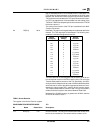
DC CHARACTERISTICS (continued)
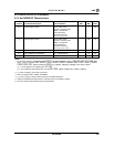
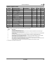
3.3 V Am79C930 DC Characteristics
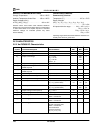
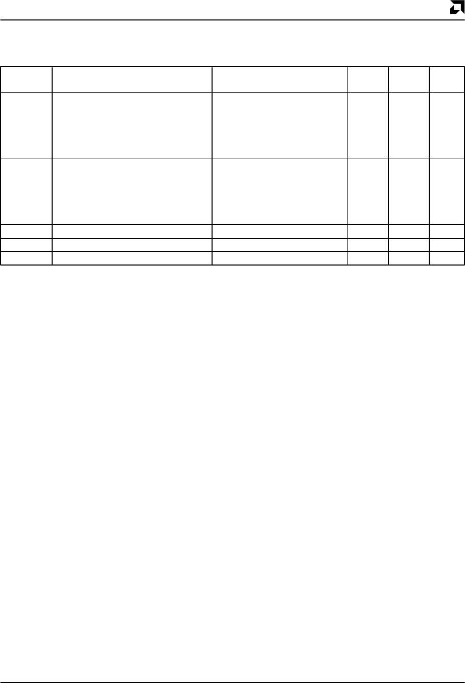
Parameter
Symbol Parameter Description Test Conditions Min Max Units
IDDPD2 Power Supply Current Power Down mode 5 mA
CLKIN = internally cutoff,
PMX1 = 32.768 kHz,
no host interface
accesses occurring
VIN ≤ VIL or VIN ≥ VOH
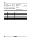
IDDPD3 Power Supply Current Power Down mode 900 µA
CLKIN = internally cutoff,
PMX1 = 32.768 kHz,
no host interface
accesses occurring
VIN ≤ VOLC or VIN ≥ VOHC
CIN Input Pin Capacitance FC = 1 MHz (Note 6) 12 pF
CO I/O or Output Pin Capacitance FC = 1 MHz (Note 6) 12 pF
CCLK BCLK Pin Capacitance FC = 1 MHz (Note 6) 12 pF
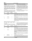
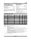
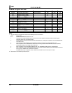
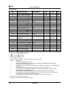
Notes:
1. I
OL1
= 2.4mA applies to the following pins:
STSCHG
, PWRDWN, MA[16:0], MD[7:0],
FCE, SCE, XCE, MOE, MWE,
TDO,
LFPE
, LFCLK, LLOCKE,
HFPE, INPACK,
HFCLK, ANTSLT,
ANTSLT,
TXCMD,
TXCMD, TXPE,
TXDATA,
TXDATA,
TXMOD, RXPE, FDET,
SDCLK, SDDATA,
SDSEL
[3:1], SAR[6:0], USER[4:2], USER[0], TXC, ADIN1, ADIN2.
I
OL2
= 12 mA applies to the following pins:
ACT, LNK
I
OL3
= 8 mA applies to the following pins: D[7:0],
WAIT, IREQ
, USER5, USER6, RXC, USER7, USER[1]
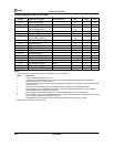
2. V
OH
does not apply to open-drain output pins.
3. Does not apply to PMX1, PMX2, and ADREF.
4. I
OZH
and I
OZL
apply to all three-state output pins and bidirectional pins.
5. Outputs are CMOS and will be driven to rail if the load is not resistive to supply.
6. Not 100% tested. Value determined by characterization.