


P R E L I M I N A R Y
AMD
39Am79C930
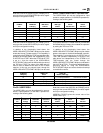
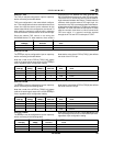
Pin 115: TXC
The TXC pin may be configured for input or output op-
eration according to the table below:
TXC input configuration is the reset default configura-
tion. This configuration allows an external transceiver to
control the clock that serves as the reference for the
transmit data. While in this configuration, the internal TX
state machine continues to operate with a reference
clock derived from a divided version of the CLKIN input.
Since the external TXC source is not driving the
Am79C930 device TX state machine, there exists a
synchronizing FIFO between the CRC generator and
the TXDATA pin that is used only in the TXC input mode.
This serial FIFO is 16 bits long and is used to allow for
slight mismatch between the internal TX state machine
reference clock and the external TXC input clock. It is
imperative in the TXC input mode that the Data Rate se-
lected with the Data Rate bits of TCR30 must match the
expected TXC clock rate from the transceiver. If these
rates do not match, then there is a risk of internal serial
FIFO error which, if it occurred, would be signaled
through the ATFU and ATFO interrupts of TCR11.
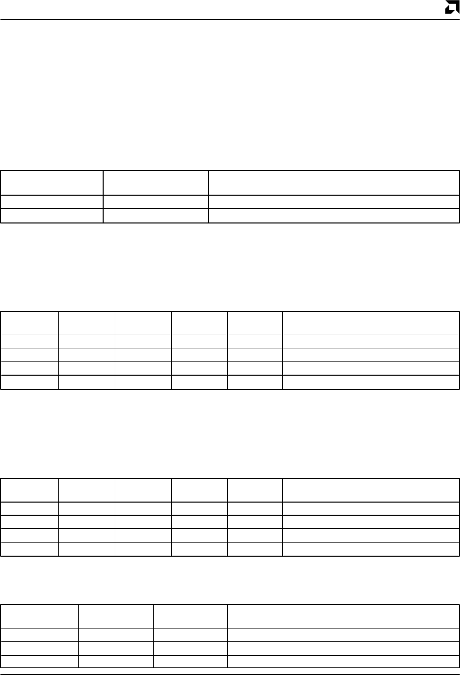
TXCIN TXC Pin TXC Pin
TCR30[3] Direction Value
0 O TXC (result of internal divide of CLKIN)
1 I NA reset default condition
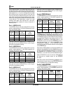
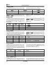
Pin 118: LFPE
The LFPE pin may be configured for input or output op-
eration according to the table below:
Note that a read of the LFPE bit (TIR0[1]) will always
yield the inverted logical sense of the current LFPE pin
value, regardless of pin configuration setting.
Note that the value of the LFPE bit (TIR0[1]) also affects
the value of the LFCLK pin.
LFPEEN LFPE CLKGT20 LFPE Pin LFPE Pin LFCLK Pin
TCR13[6] TIR0[1] MIR9[7] Direction Value Value
0 X X I NA LOW
1 0 X O HIGH LOW reset default condition
1 1 0 O LOW CLKIN
1 1 1 O LOW CLKIN÷2
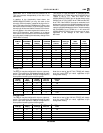
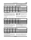
Pin 120: HFPE
The HFPE pin may be configured for input or output op-
eration according to the following table:
Note that a read of the HFPE bit (TIR0[0]) will always
yield the inverted logical sense of the current HFPE pin
value, regardless of pin configuration setting.
Note that the value of the HFPE bit (TIR0[0]) also affects
the value of the HFCLK pin.
HFPEEN HFPE CLKGT20 HFPE Pin HFPE Pin HFCLK Pin
TCR13[5] TIR0[0] MIR9[7] Direction Value Value
0 X X I NA LOW
1 0 X O HIGH LOW reset default condition
1 1 0 O LOW CLKIN
1 1 1 O LOW CLKIN÷2
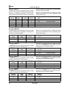
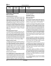
Pin 122: RXPE
The RXPE pin may be configured for input or output op-
eration according to the following table:
Note that a read of the RXP bit (TIR0[2]) will always yield
the inverted logical sense of the current RXPE pin value,
regardless of pin configuration setting.
RXPELEN RXP RXPE Pin RXPE Pin
TCR13[0] TIR0[2] Direction Value
0XI NA
1 0 O HIGH reset default condition
1 1 O LOW