


Am79C930 17
PRELIMINARY
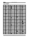
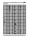
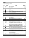
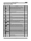
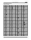
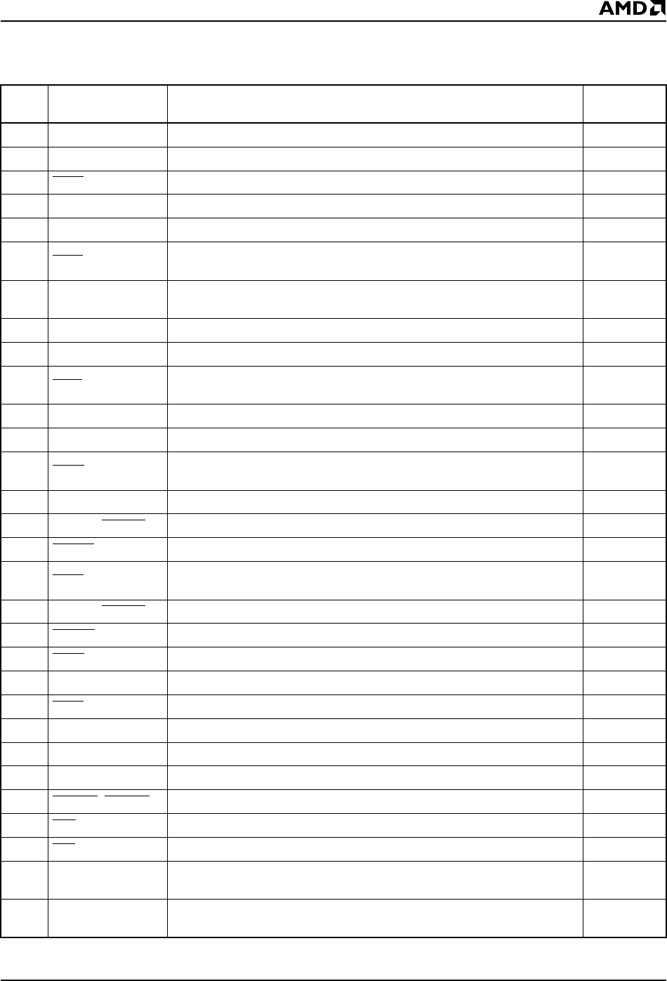
PCMCIA PIN FUNCTION SUMMARY (continued)
PCMCIA Pin Summary (continued)
No. of
Pins Pin Name Pin Function Pin Style
1 TDO Test Data Out—this is the data output signal for IEEE 1149.1 testing TS1
1 TMS Test Mode Select—this is the test mode select for IEEE 1149.1 testing I
1 TRST
Test Reset—this is the reset signal for IEEE 1149.1 testing I
1 USER7 User-programmable pin PTS3
1 RXC Receive Clock—provides decode receive clock PTS3
1 TEST
Test pin—when asserted, this pin places the Am79C930 device into a
nonstandard factory-only test mode
I
1 CLKIN
Clock input to drive BIU, 80188 core, and TAI, supplying network data rate
information
I
2 PMX1–2 Power Management Xtal—32-kHz Xtal input for sleep timer reference I/XO
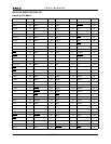
1 TXC Transmit Clock—may be configured either as input or output TS1
1 LFPE
Low Frequency Power Enable—used to power up the low-frequency section of
the transceiver
PTS1
1 LFCLK Low Frequency Clock—a reference signal for the transceiver synthesizer TS1
1 LLOCKE Low Frequency Synthesizer Lock—a programmable signal PTS1
1 HFPE
High Frequency Power Enable—used to power up the high-frequency section
of the transceiver
PTS1
1 HFCLK High Frequency Clock—a reference signal for the transceiver synthesizer TS1
2 ANTSLT, ANTSL
T Antenna Select—used to select between two antennas PTS1
2 TXCMD, TXCMD Transmit Command—used to select the transmit path in the transceiver TP1, PTS1
1 TXPE
Transmit Power Enable—used to power up the transmit section of the
transceiver
TP1
2 TXDATA, TXD
ATA Transmit Data—supplies the transmit data stream to the transceiver TP1, PTS1
1 TXMOD Transmit Modulation Enable—enables the modulation of transmit data TP1
1 RXPE Receive Power Enable—enables the receive function of the transceiver PTS1
1 RXDATA Receive Data—accepts receive data in NRZ format from the transceiver I
1 FDET Frame Detect—start of frame delimiter detection indication TS1
1 RXCIN Receive Clock Input—optional clock input that allows for an external PLL IPU
1 SDCLK Serial Data Clock—clock output used to access serial peripheral devices PTS1
1 SDDATA Serial Data Data—data pin used to access serial peripheral devices PTS1
3 SDSEL3–SDSEL1 Serial Data Select—chip select outputs used to select serial peripheral devices PTS1
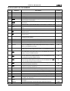
1 ACT Activity LED—output capable of driving an LED PTS2
1 LNK Link LED—output capable of driving an LED PTS2
1 ADREF
A/D Reference—an input that can be used to set the analog reference voltage
for the internal A/D converter
I
7 SAR6–SAR0
Serial Approximation Register—supplies the value of the serial approximation
register used in the A/D converter
TS1