P R E L I M I N A R Y
AMD
63Am79C930
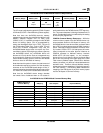
The following table indicates the mapping of all I/O re-
sources that are accessible through the Am79C930
PCMCIA system interface. Note that some resources
are physically located within the BIU, while others are lo-
cated in the TAI and still others exist as external Flash
and SRAM:
Am79C930 Device PCMCIA Mode I/O MAP
Resource Resource PCMCIA Resource Physical Location
Name Mnemonic I/O Address SIR1[2:0] Size of Resource
SIR0: General SIR0: GCR 00h XXX* 1 byte BIU
Configuration Register
SIR1: Bank Switching SIR1: BSS 01h XXX 1 byte BIU
Select Register
SIR2: Local Memory SIR2: LMAL 02h XXX 1 byte BIU
Address [7:0]
SIR3: Local Memory SIR3: LMAU 03h XXX 1 byte BIU
Address [14:8]
SIR4: I/O Data SIR4: DPLL 04h XXX 1 byte Indirect access to
Port[7:0] SRAM or Flash
memory
SIR5: I/O Data SIR5: DPLM 05h XXX 1 byte Indirect access to
Port[15:8] SRAM or Flash
memory
SIR6: I/O Data SIR6: DPUM 06h XXX 1 byte Indirect access to
Port [23:16] SRAM or Flash
memory
SIR7: I/O Data SIR7: DPUU 07h XXX 1 byte Indirect access to
Port [31:24] SRAM or Flash
memory
TIR 0–7 – 08h – 0Fh 000 1 byte TAI
each location
TIR 8–15 – 08h – 0Fh 001 1 byte TAI
each location
TIR 16–23 – 08h – 0Fh 010 1 byte TAI
each location
TIR 24–31 – 08h – 0Fh 011 1 byte TAI
each location
UNDEFINED – 10h – 3Fh 0XX NA UNDEFINED
TIR 0–31 – 08h – 27h 1X 1 byte TAI
each location
UNDEFINED – 28h – 3Fh 1XX NA UNDEFINED
*X = Don’t Care
ISA Plug and Play Mode Resources
The Am79C930 device fully supports the ISA Plug
and Play specification, revision 1.0a, including the
Plug and Play ADDRESS Auto-configuration port,
WRITE_DATA Auto-configuration port, READ_DATA
Auto-configuration port, and 19 of the Plug and Play
configuration registers, as well as providing a mecha-
nism for access to Flash memory for reading the
Am79C930 device’s Plug and Play Resource Data.
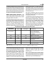
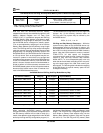
The following table indicates the range of I/O and mem-
ory addresses to which the Am79C930 device will re-
spond when operating in the ISA Plug and Play mode.


