


AMD
P R E L I M I N A R Y
128
Am79C930
ABSOLUTE MAXIMUM RATINGS
Storage Temperature: –65 to +150°C. . . . . . . . . . . .
Ambient Temperature Under Bias: –65 to +125°C. . .
Supply Voltage to AVSS
or DVSS (AVDD, DVDD): –0.3 to +6 V. . . . . . . . . . . . . .
Stresses above those listed under Absolute Maximum
Ratings may cause permanent device failure. Functionality at
or above these limits is not implied. Exposure to Absolute
Maximum Ratings for extended periods may affect
device reliability.
OPERATING RANGES
Commercial (C) Devices
Temperature (T
A)0°C to + 70°C. . . . . . . . . . . . . . . . .
Supply Voltages (AV
DD, VCC, VDDT, VDDU1, VDDU2, VDDM,
V
DDP, VDD5) 3.0 V to 3.6 V. . . . . . . . . . . . . . . . . . . . . .
Supply Voltages
(AV
DD, VDD5) +5 V ± 5%. . . . . . . . . . . . . . . . . . . . . . . .
All inputs within the range: AV
SS – 0.5 V ≤ VIN ≤. . . . .
AV
DD + 0.5 V, or
DV
SS – 0.5 V ≤ VIN ≤
DV
DD + 0.5 V
Operating ranges define those limits between which the func-
tionality of the device is guaranteed.
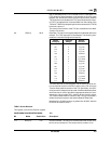
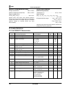
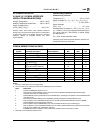
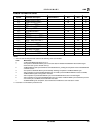
3.3 V Am79C930 DC CHARACTERISTICS
Parameter
Symbol Parameter Description Test Conditions Min Max Units
VIL Input LOW Voltage –0.3 0.8 V
VIH Input HIGH Voltage 2.0 VDD + 0.3 V
VOL Output LOW Voltage IOL1 = 2.4 mA 0.4 V
IOL2 = 12 mA 0.4
IOL3 = 8 mA 0.4
(Note 1, 5)
VOH Output HIGH Voltage (Note 2) IOH = –0.4 mA (Note 5) 2.4 V
VOLC Output LOW Voltage for IOL = 0.2 mA V
CMOS only load
VOHC Output HIGH Voltage for IOL = –0.2 mA VDD – 0.2 V
CMOS only load
IIX Input Leakage Current (Note 3) VDD = 5 V, VIN = 0 V –10 10
µA
VILX XTAL1 Input LOW Voltage Threshold VIN = External Clock –0.5 0.8 V
VIHX XTAL1 Input HIGH Voltage Threshold VIN = External Clock 3.5 VDD + 0.5 V
IILX XTAL1 Input LOW Current VIN = External Clock (Active) –100
µA
VIN = DVSS (Power Down) –10 +10
µA
IIHX XTAL1 Input HIGH Current VIN = External Clock (Active) 100
µA
VIN = VDD (Power Down) 400
µA
IOZL Output Leakage Current (Note 4) VOUT = 0.4 V –10 µA
IOZH Output Leakage Current (Note 4) VOUT = VDD 10 µA
IDDF Power Supply Current CLKIN = 40 MHz, 105 mA
PMX1 = 32.768 kHz
IDDS Power Supply Current CLKIN = 20 MHz, 60 mA
PMX1 = 32.768 kHz
IDDPD1 Power Supply Current Power Down mode 15 mA
CLKIN = internally cutoff,
PMX1 = 32.768 kHz,
no host interface
accesses occurring
VIN ≤ VIL or VIN ≥ VIH