


P R E L I M I N A R Y
AMD
51Am79C930
values were found to be correct. These register values
can be used to determine the end of a received frame.
When good CRC values are found, these may be sig-
naled to the 80188 core through interrupt bits in TIR5.
The CRC32 polynomial is X32+X26+X23+X22+X16
+X12+X11+X10+X8+X7+X5+X4+X2+X+1; the initial
condition of the CRC32 calculation is FFFF FFFFh; and
the final remainder of the CRC32 operation is
DEBB 20E3h.
The CRC8 polynomial is X8+X5+X+1; the initial condi-
tion of the CRC8 calculation is FFh; and the final ex-
pected remainder of the CRC8 operation is 66h.
RX Status Reporting
TIR11 provides bits that indicate the current state of the
Am79C930 device with respect to the reception of a
frame. For example, the TIR11 bits indicate the number
of bytes currently in the RX FIFO and whether or not a
reception is active.
Bit Ordering
Both Big and Little Endian support is available for trans-
mit and receive operations. The default mode is Little
Endian. The operational mode is selected with the WNS
bit of TCR3. Only FIFO data is affected by the WNS set-
ting. No other register information is swapped.
RSSI A/D Unit
Several modes of operation are possible with the
Am79C930 A/D subunit. The following two paragraphs
describe the basic internal mode of operation. Following
this description is a list of the additional modes and de-
scriptions of each. For programming information, refer
to the ADDA bit description under TIR26[2].
The TAI contains a configurable RSSI A/D unit that al-
lows externally supplied analog values to be converted
to 7-bit digital values. Two A/D analog input pins are pro-
vided (ADIN1, ADIN2). The active input may be selected
with the SRCS (Source Select) bit in TIR26. The conver-
sion time of the internal A/D converter is approximately
600 ns. The frequency of sample conversion is con-
trolled with the Antenna Diversity Timer register
(TCR4). A/D converter output values are available at the
SAR[6:0] output pins for external use. A/D converter
output values are available to firmware by reading from
TIR27. The result of the A/D conversion is used by inter-
nal logic to perform Clear Channel Assessment (CCA)
and Antenna Diversity tests. A reference input (ADREF)
is supplied which allows the user to set the upper range
limit on the A/D converter.
The RSSI A/D unit’s output may be used by the CCA
logic and by the Antenna Diversity logic, depending
upon the setting of the URSSI bit of TCR28. If the URSSI
bit is set to 1, then the A/D conversion process begins
after a programmable delay following an antenna
diversity antenna switching operation. (The switching
operation is periodic, with the period being set with the
Antenna Diversity Timer register of TCR4.) The delay
from antenna switch to the beginning of the A/D conver-
sion operation is programmed in the RSSI Sample Start
register (TCR24). The converted RSSI value is then
compared against the RSSI Lower Limit value that is
programmed into TIR28. The current RSSI limit com-
parison test result may be read from the RSALT bit
(RSSI Above Limit) of TIR28. The result of this compari-
son test is fed to the CCA decision logic and to the Stop
Diversity decision logic when the URSSI bit of TCR28 is
set to 1.
There are three submodes to the basic internal A/D
converter mode:
Internal_A mode disables the SAR pins (TCR25[5] =
ENSAR = 0)
Internal_B mode allows the converted value to be
driven onto the SAR pins. (TCR25[5] = ENSAR = 1)
Internal_C mode allows an external circuit to control
the timing of the A/D sample and convert operation in
order to synchronize the internal Am79C930 de-
vice’s A/D operation with the operations of an exter-
nal antenna selection scheme. This mode is
selected with the UXA2DST bit of TCR25[7].
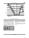
Normally, the A/D conversion starts when the Antenna
Dwell Timer counts down to the value programmed in
the Sample Start field of TCR24 (SS field). The antenna
dwell timer repeats its cycle every ADT[5:0] time steps,
forever. If a satisfactory antenna is found, then the an-
tenna switching ceases, but RSSI testing continues to
provide input to the CCA logic at the end of each “dwell.”
However, when UXADTST is set to 1, then the A/D con-
verter will sample and convert whenever a rising edge
appears on the USER6/IRQ5/EXTSDF/EXTA2DST pin.
The conversion process will occur over the time pro-
grammed in the TCR25 A2DT field. This function allows
an external circuit to synchronize the function of the
Am79C930 A/D converter to the external circuit’s peri-
odic requirements. A/D converted values will be avail-
able on the SAR output pins, provided that the ENSAR
bit of TCR25 has been set to a 1.
In addition to the internal A/D modes, there are two ex-
ternal modes, one for A/D and one for D/A:
External A/D mode causes the ADIN1 and ADIN2 pins
to become outputs, which are then used to control the
power cycling and conversion of an external A/D device.
The SAR pins are used as inputs in this mode to allow
the externally converted value to be driven back into the
Am79C930 device, so that it may be used in the CCA
and Antenna Diversity logic circuits. In this mode,
ADIN1 functions as the power control signal. ADIN1 be-
comes active at the beginning of the A/D cycle, with a
period as specified in the Antenna Diversity Timer