


iii
1.31 DC Gear Holder Assy............................................................................................. IV-6
1.31.1 Scanner Fan Motor .................................................................................. IV-6
1.32 PS Switch Wire, Remote Switch ........................................ Refer to HL-1260 (P.IV-23)
1.33 High-Voltage Power Supply PCB Assy............................... Refer to HL-1260 (P.IV-24)
1.34 Low-Voltage Power Supply PCB Assy ............................... Refer to HL-1260 (P.IV-24)
1.35 Toner Cartridge (EP-ED Cartridge) .................................... Refer to HL-1260 (P.IV-25)
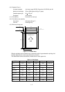
1.36 Paper Tray ............................................................................................................. IV-7
CHAPTER V MAINTENANCE AND SERVICING
1. PERIODICAL REPLACEMENT PARTS .......................................... Refer to HL-1260 (P.V-1)
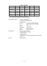
2. CONSUMABLE PARTS STANDARD ENDURANCE TABLE ............................................ V-1
3. LIST OF STANDARD TOOLS ......................................................... Refer to HL-1260 (P.V-2)
4. LIST OF LUBRICANTS AND CLEANERS ...................................... Refer to HL-1260 (P.V-3)
CHAPTER VI TROUBLESHOOTING
1. INTRODUCTION ............................................................................ Refer to HL-1260 (P.VI-1)
1.1 Initial Check.......................................................................... Refer to HL-1260 (P.VI-1)
1.2 Basic Procedure ................................................................... Refer to HL-1260 (P.VI-2)
2. TEST PRINTING AND MECHANICAL CHECK .............................. Refer to HL-1260 (P.VI-2)
2.1 Test Printing ......................................................................... Refer to HL-1260 (P.VI-2)
3. IMAGE DEFECTS .......................................................................... Refer to HL-1260 (P.VI-3)
3.1 Image Defect Examples ....................................................... Refer to HL-1260 (P.VI-3)
3.2 Troubleshooting Image Defects ........................................... Refer to HL-1260 (P.VI-4)
4. TROUBLESHOOTING OF MALFUNCTIONS .................................................................. VI-1
5. TROUBLESHOOTING PAPER TRANSPORT PROBLEMS......... Refer to HL-1260 (P.VI-19)
5.1 Paper Jams ........................................................................ Refer to HL-1260 (P.VI-19)
5.2 Incomplete Paper Feed ...................................................... Refer to HL-1260 (P.VI-22)
6. OPERATION ................................................................................ Refer to HL-1260 (P.VI-23)
6.1 Line Inspection Mode Procedure ....................................... Refer to HL-1260 (P.VI-23)
6.2 DRAM Test ......................................................................... Refer to HL-1260 (P.VI-25)
7. STATUS MESSAGE LIST ................................................................................................VI-9
APPENDICES
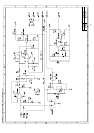
1. Engine Block Diagram ....................................................................................................... A-1
2. Paper Feed/Size-SW PCB Circuitry Diagram (1/1)........................... Refer to HL-1260 (P.A-2)
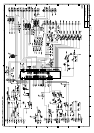
3. Main PCB Circuitry Diagram (1/7) ..................................................................................... A-2
4. Main PCB Circuitry Diagram (2/7) ..................................................................................... A-3
5. Main PCB Circuitry Diagram (3/7) ..................................................................................... A-4
6. Main PCB Circuitry Diagram (4/7) ..................................................................................... A-5
7. Main PCB Circuitry Diagram (5/7) ..................................................................................... A-6
8. Main PCB Circuitry Diagram (6/7) ..................................................................................... A-7
9. Main PCB Circuitry Diagram (7/7) ..................................................................................... A-8
10. Control Panel PCB Circuitry Diagram (1/1) ....................................Refer to HL-1260 (P.A-11)
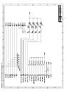
11. Scanner LD PCB Circuitry Diagram (1/1) .......................................................................... A-9