III - 3
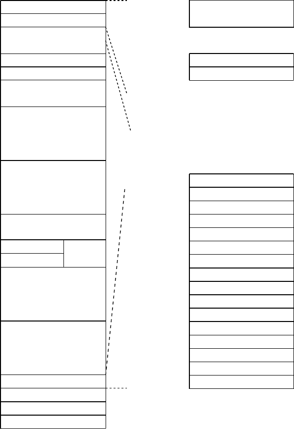
3) The attached Printer SIMM map shows the memory map for 2 SIMMs combined.
(6) ROM block
ROMs store the CPU control program and font data. ROMs are two 16Mbit masked ROMs and
two 8Mbit masked ROMs.
Optional sockets are available for two 8Mbit EPROM (µPD27C8000DZ-120 - NEC or equiva-
lent) for expansion.
ROM access time should be less than 120nsec.
8Mbit EPROMs can be used instead of a 16Mbit masked ROM.
(7) DRAM block
DRAMs are used for receiving buffer or working area of the CPU. The DRAM block contains
four 4Mbit DRAMs, thus having 2MB memory capacity in total.
The refreshing method is CBR (Cas Before Ras).
DRAM access time should be less than 80nsec.
$0000-0000
$0000-0000
$003F-FFFF
$0040-0000
$0060-0000
$007F-FFFF
$1C00-0000
$1CFF-FFFF
$0400-0000
$0410-0000
$0800-0000
$0C00-0000
$1000-0000
$13C0-0000
$13E0-0000
$1400-0000
$1800-0000
$1C00-0000
$1D00-0000
$1F00-0000
$1FFF-FFFF
$1E00-0000
ROMOA, OB, 1A, 1B
Program ROM
(4MB)
Font ROM (2MB)
Optional ROM (2MB)
SELROM0(External battery terminal)
SELROM1(External battery termial)
ROM1B
Not used
MIO
MIO-EOT
FC
(64 MB)
FC
(64MB)
SIMM
(max64MB)
Reserve
(64MB)
ASIC internal register
Gate Array (16MB)
CDCC read buffer
BOOT-ROM
IRASO
Not used
Built-in RAM2MB
Soft Support Function
Timer
Serial
CDCC
MED Relation
Not used
HRC/GSC
Memory Wait Control
Interrupt control
Interrupt mask
Memory bank
LSB control
LSB setting
CPU write for LSB
Not used
Not used
Figure 3.2 Memory Map


