


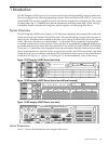
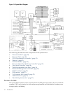
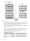

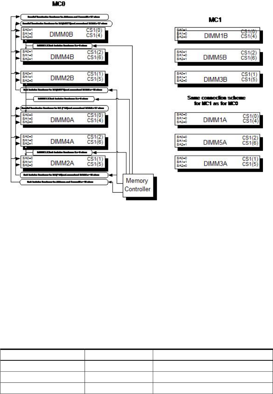
Figure 1-5 Memory Block Diagram
Memory Architecture
The I/O ASIC memory interface supports two DDR cells. Each cell is 144 data bits wide. The
memory subsystem physical design uses a comb-filter termination scheme for the data and the
address and control buses. This topology is similar to other DDR designs. Clocks are distributed
directly from the I/O ASIC. Each clock pair drives two DIMMs.
Memory data is protected by the ECC. Eight ECC bits per DIMM protect 64 bits of data. The use
of ECC allows correction of single-bit errors, and detection of multi-bit errors. Only DIMMs with
ECC are qualified or supported.
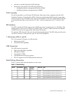
DIMMs
The memory subsystem supports only DDR SDRAM (Double Data Rate Synchronous Dynamic
Random Access Memory) technology utilizing industry-standard PC-1600 type DDR SDRAM
DIMMs, 1.2" tall. The DIMMs use a 184-pin JEDEC standard connector.
DIMMs are loaded in a group of four, known as a quad. All four DIMMs in a quad must be the
same size. Table 1-2 summarizes the memory solutions.
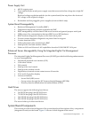
Table 1-2 Memory Array Capacities
DDR SDRAM Count, Type, and TechnologySingle DIMM SizeMininum/Maximum Memory Size
18 x 32 MB x 4 DDR1 SDRAMs (128 MB)256 MB DIMM1 GB / 3 GB
36 x 32 MB x 4 DDR1 SDRAMs (128 MB)512 MB DIMM2 GB / 6 GB
36 x 64 MB x 4 DDR1 SDRAMs (256 MB)1024 MB DIMM4 GB / 12 GB
24 Introduction