Chapter 5 Calibration
© National Instruments Corporation 5-3 Lab-NB User Manual
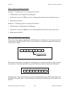
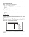
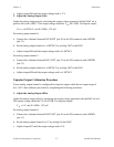
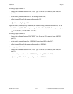
Analog Input Calibration
To null out error sources that compromise the quality of measurements, you must calibrate the
analog input circuitry by adjusting the following potential sources of error:
• Offset errors
• Gain error of the analog input circuitry
The calibration must be performed if the input configuration is changed from bipolar (the factory
setting) to unipolar.
Offsets at the input to the instrumentation amplifier contribute gain-dependent offset error to the
analog input circuitry. This offset is multiplied by the gain instrumentation amplifier. Other
sources of offset error include the track-and-hold amplifier and the ADC. On the Lab-NB, one
trimpot is used to null out all of these offset sources. Because one of these error sources is gain-
dependent, the offset should be checked and recalibrated, if necessary, whenever the gain is
changed significantly. Alternatively, the input offset calibration can be performed at gain = 1
with the offset errors noted for all other gains. A software correction can then be applied to the
readings at gains higher than one by subtracting the offset errors. Using this method, the board
can be used at all available gain levels without recalibrating the input.
The maximum offset at the gain amplifier is specified at 0.5 mV. The gain amplifier's maximum
possible contribution to the total offset is therefore 0.5 mV multiplied by the gain. To find the
error in LSBs, divide this voltage by the voltage of 1 LSB. Hence, with a large gain change,
such as from 1 to 100, the number of LSBs of offset from this source changes from about 0.2 to
almost 20. Clearly, an adjustment that is acceptable for a 0.2 LSB error is probably not suitable
when the error is multiplied by 100. For small changes in the gain, the error that accompanies
changes in gain is much less. If the gain is changed from 1 to 2 or 5, the offset probably does not
need to be recalibrated. Likewise, changes between gains of 20, 50, or 100 probably do not
require recalibration.
All the stages up to and including the input to the ADC contribute to the gain error of the analog
input circuitry. With the amplifier set to a gain of 1, the gain of the analog input circuitry is
ideally 1. The gain error is the deviation of the gain from 1 and appears as a multiplication of the
input voltage being measured. To calibrate this offset, you must apply V
+fs
-1.5 LSB to the
analog input circuitry and adjust a potentiometer until the ADC returns readings that flicker
between its most positive count and the most positive count minus 1. The voltages
corresponding to V
+fs
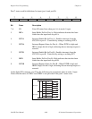
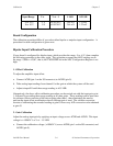
and 1 LSB are given in the following table.
The voltages corresponding to V
-fs
, which is the most negative voltage that the ADC can read,
V
+fs
- 1, which is the most positive voltage the ADC can read, and 1 LSB, which is the voltage
corresponding to one count of the ADC, depend on the input range selected. The value of these
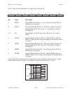
voltages for each input range is given in the following table.


