


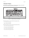
Specifications Appendix A
Lab-NB User Manual A-2 © National Instruments Corporation
normally called nonlinearity, because relative accuracy ensures that the sum of quantization uncertainty and A/D
conversion error does not exceed a given amount.
Integral nonlinearity in an ADC is an often ill-defined specification that is supposed to indicate a converter's overall
A/D transfer linearity. The manufacturers of the ADC chips used by National Instruments specify their integral
nonlinearity by stating that the analog center of any code will not deviate from a straight line by more than
±
1
/2 LSB. This specification is misleading because although a particularly wide code's center may be found within
±
1
/2 LSB of the ideal, one of its edges may be well beyond ±1 LSB. Thus, the ADC has a relative accuracy of that
amount. National Instruments tests its boards to ensure that they meet all three linearity specifications defined in
this appendix; specifications for integral nonlinearity are included primarily to maintain compatibility with a
convention of specifications used by other board manufacturers. Relative accuracy, however, is much more useful.
Differential nonlinearity is a measure of deviation of code widths from their theoretical value of
1 LSB. The width of a given code is the size of the range of analog values that can be input to produce that code,
ideally 1 LSB. A specification of ±1 LSB differential nonlinearity ensures that no code has a width of 0 LSBs (that
is, no missing codes) and that no code width exceeds 2 LSBs.
System noise is the amount of noise seen by the ADC when there is no signal present at the input of the board. The
amount of noise that is reported directly (without any analysis) by the ADC is not necessarily the amount of real
noise present in the system, unless the noise is ≥ 0.5 LSB RMS. Noise that is less than this magnitude produces
varying amounts of flicker, and the amount of flicker seen is a function of how near the real mean of the noise is to a
code transition. If the mean is near or at a transition between codes, the ADC flickers evenly between the two
codes, and the noise is seen as very nearly 0.5 LSB. If the mean is near the center of a code and the noise is
relatively small, very little or no flicker is seen, and the noise is reported by the ADC as nearly 0 LSB. From the
relationship between the mean of the noise and the measured RMS magnitude of the noise, the character of the noise
can be determined. National Instruments has determined that the character of the noise in the Lab-NB is fairly
Gaussian, and so the noise specifications given are the amounts of pure Gaussian noise required to produce our
readings.
Analog Data Acquisition
Data transfers................................................................................Programmed I/O or interrupts
Max sample rate..........................................................................62.5 kHz
Analog bandwidth (-3 dB).......................................................400 kHz (gain = 1)
40 kHz (gain = 100)
Max multichannel scan rate....................................................62.5 kHz (gain = ≤ 50)
20 kHz (gain = 100)
Analog Output
Number of output channels.....................................................2 single-ended
Analog resolution........................................................................12 bits, one part in 4,096
Relative accuracy (nonlinearity)...........................................±0.75 LSB max
Differential nonlinearity...........................................................±1 LSB max (monotonic over temperature),
±0.25 LSB typ
Offset adjustment range, min.................................................±37 mV
Gain adjustment range, min....................................................±39 mV
Output voltage ranges................................................................0 to +10 V, unipolar mode
±5 V, bipolar mode; software selectable
Current drive capability............................................................±1 mA
Output settling time...........................................................7 µsec for 10 V step to 0.012%
Output slew rate..................................................................9 V/µsec
Output Impedance.......................................................................0.1 Ω max
Temperature coefficients
Gain error..............................................................................±10 ppm/° C