


Calibration Chapter 5
Lab-NB User Manual 5-4 © National Instruments Corporation
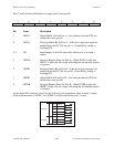
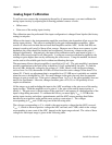
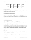
Input Range V
-fs
V
+fs
- 1 1 LSB 0.5 LSB
-5 to +5 V -5 V +4.99756 V 2.44 mV 1.22 mV
0 to 10 V 0 V +9.99756 V 2.44 mV 1.22 mV
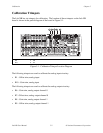
Board Configuration
The calibration procedure differs if you select either bipolar or unipolar input configuration. A
procedure for each configuration is given next.
Bipolar Input Calibration Procedure
If your board is configured for bipolar input, which provides the range -5 to +5 V, then complete
the following procedure in the order given. This procedure assumes that ADC readings are in
the range -2,048 to +2,047, that is, the TWOSCMP bit in the ADC Configuration Register is set
high.
1. Offset Calibration
To adjust the amplifier input offset:
a. Connect ACH0 (pin 1 on the I/O connector) to AGND (pin 9).
b. Take analog input readings from channel 0 at the gain at which the system will be used.
c. Adjust trimpot R1 until the average reading is ±0.5 LSB.
Alternatively, the above offset calibration procedure can be carried out with the input gain set at
1, followed by recording the average reading at all other gains. These readings can be used later
for software offset correction of the data at gains other than 1, thus eliminating the need to
perform the input offset recalibration when a different gain is used. The software correction
consists of subtracting the recorded reading at gain G from every A/D conversion value obtained
at gain G.
2. Gain Calibration
Adjust the analog input gain by applying an input voltage across ACH0 and AGND. This input
voltage is +4.99634 V or V
+fs
- 1.5 LSB.
a. Connect the calibration voltage (+4.99634 V) across ACH0 (pin 1 on the I/O connector) and
AGND (pin 9).