Chapter 3 Theory of Operation
© National Instruments Corporation 3-3 Lab-NB User Manual
The starting-address-detecting circuitry on the Lab-NB matches address lines 23 through 21 to
the starting address specified by the slot in which the Lab-NB board is installed. The remaining
address lines (19 through 0) are decoded by the Lab-NB address-decoding circuitry to generate
select signals for the registers on the board. The NuBus interface timing signals are decoded by
the Lab-NB interface timing circuitry, which generates the proper read and write signals for the
remaining Lab-NB circuitry. The Lab-NB board can cause interrupts in the Macintosh by
driving the NuBus NMRQ* interrupt line.
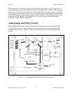
Analog Input and DAQ Circuitry
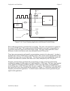
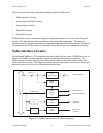
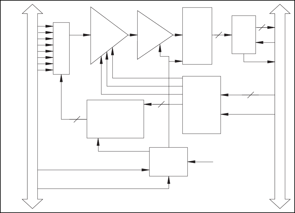
The Lab-NB provides eight channels of analog input with software-programmable gain and
12-bit A/D conversion. Using the timing circuitry, the Lab-NB can also automatically time
multiple A/D conversions. Figure 3-3 shows a block diagram of the analog input and DAQ
circuitry.
Sample-
and-Hold
Amp
NuBus
Mux
Counter
Data
Acquisition
Timing
ADC
Configuration
Register
Mux
Pro-
grammable
Gain Amp
ADC
A/D
FIFO
MUX CTR CLK
External Trigger
Counter/Timer
Signals
ADC WR
CONV
AVAIL
A/D
RD
EXT
CONV*
EXT
TRIG
ACH0
ACH1
ACH2
ACH3
ACH4
ACH5
ACH6
ACH7
12
12
16
3
4
A/D
Data
Data
Data
MUX
OUT
I/O Connector
GAIN0
GAIN1
GAIN2
Convert
Figure 3-3. Analog Input and DAQ Circuitry Block Diagram


