Chapter 4 Register-Level Programming
© National Instruments Corporation 4-15 Lab-NB User Manual
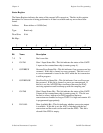
DAC0 and DAC1 Data Registers
Writing to these registers loads the corresponding analog output channel DAC, thereby updating
the voltages generated by the analog output channels. The voltage is updated immediately,
unless the TMRWGN bit for that DAC is set. If this bit is set, then the voltages are not updated
until the next pulse from counter A2 or the next low-to-high transition on the EXTUPDATE*
line on the I/O connector. If the timer interrupt enable bit (TMRINTEN) in the Interrupt Status
Register is set, then a write to any one of these registers will service that interrupt and clear
TMRINTEN.
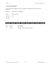
Address: Base address + 5 8010 (hex) Load DAC0.
Base address + 5 8020 (hex) Load DAC1.
Base address + 5 8030 (hex) Load DAC0 and DAC1 simultaneously.
Type: Write-only
Word Size: 16-bit
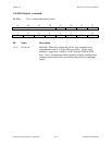
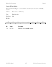
Bit Map:
15 14 13 12 11 10 9 8
X X X X D11 D10 D9 D8
76543210
D7 D6 D5 D4 D3 D2 D1 D0
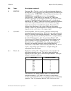
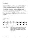
Bit Name Description
15–12 X Don’t care bits.
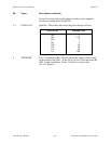
11–0 D<11..0> Data Bit—These 12 bits are loaded into the specified DAC,
thereby updating the voltage generated by the analog output
channel (see Programming the Analog Output Circuitry later in
this chapter for a table mapping digital values to output voltage).


