Theory of Operation Chapter 3
Lab-NB User Manual 3-4 © National Instruments Corporation
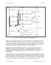
Analog Input Circuitry
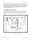
The analog input circuitry consists of an input multiplexer, a software-programmable gain
amplifier, a 12-bit ADC, and a 12-bit FIFO memory that is sign-extended to 16 bits.
The input multiplexer is made up of a CMOS analog input multiplexer and has eight analog input
channels (channels 0 through 7). The input multiplexers provide input overvoltage protection of
±45 V, powered on or off.
The programmable gain amplifier applies gain to the input signal, allowing an input analog
signal to be amplified before being sampled and converted, thus increasing measurement
resolution and accuracy. The gain of the instrumentation amplifier is selected under software
control. The Lab-NB board provides gains of 1, 2, 5, 10, 20, 50, and 100.
The Lab-NB uses a 12-bit successive-approximation ADC. The 12-bit resolution of the
converter allows the converter to resolve its input range into 4,096 different steps. This
resolution also provides a 12-bit digital word that represents the value of the input voltage level
with respect to the converter input range. The ADC itself has a single input range of 0 to +5 V.
Additional circuitry allows inputs of ±5 V or 0 to 10 V.
When an A/D conversion is complete, the ADC clocks the result into the A/D FIFO. The A/D
FIFO is 16 bits wide and 16 words deep. This FIFO serves as a buffer to the ADC and provides
two benefits. First, any time an A/D conversion is complete, the value is saved in the A/D FIFO
for later reading, and the ADC is free to start a new conversion. Secondly, the A/D FIFO can
collect up to 16 A/D conversion values before any information is lost, thus allowing software
some extra time (16 times the sample interval) to catch up with the hardware. If more than 16
values are stored in the A/D FIFO without the A/D FIFO being read from, an error condition
called A/D FIFO Overflow occurs and A/D conversion information is lost.
The A/D FIFO generates a signal that indicates when it contains A/D conversion data. The state
of this signal can be read from the Lab-NB Status Register.
The output from the ADC can be interpreted as either straight binary or two's complement,
depending on which input mode you select (unipolar or bipolar). In unipolar mode, the data
from the ADC is interpreted as a 12-bit straight binary number with a range of 0 to +4,095. In
bipolar mode, the data from the ADC is interpreted as a 12-bit two's complement number with a
range of -2,048 to +2,047. In this mode, the MSB of the ADC result is inverted to make it two's
complement. The output from the ADC is then sign-extended to 16 bits, causing either a leading
0 or a leading F (hex) to be added, depending on the coding and the sign. Thus, data values read
from the FIFO are 16 bits wide.
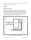
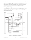
DAQ Timing Circuitry
A DAQ operation refers to the process of taking a sequence of A/D conversions with the sample
interval (the time between successive A/D conversions) carefully timed. The DAQ timing
circuitry consists of various clocks and timing signals that perform this timing. Two types of
data acquisition can be performed by the Lab-NB board: single-channel data acquisition and


