


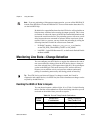

© National Instruments Corporation 3-1 653X User Manual
3
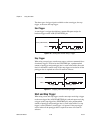
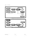
Timing Diagrams
This chapter contains timing diagrams for the handshaking and pattern I/O
modes. You can use these diagrams to get a detailed understanding about
what happens in hardware when using these modes.
Note
All timing diagrams are in nanoseconds.
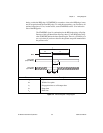
Pattern I/O Timing Diagrams
Use pattern I/O to transfer data at a timed interval upon the rising or falling
edge of the REQ signal. The REQ signal can be generated internally by the
653X device or supplied externally via the I/O connector.
Note
Your transfer rate is limited by the minimum available bus bandwidth in your
computer system, unless you are using the PCI/PXI-6534 device, which has onboard
memory. Otherwise, you are limited by the number of other devices utilizing the bus and
your application software, both of which can lower your transfer rate. For more
information about transfer rates, see Appendix E, Optimizing Your Transfer Rates.
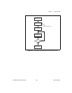
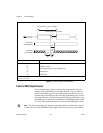
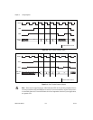
Internal REQ Signal Source
The 653X can internally generate a signal (REQ) with which to strobe data.
To program the frequency of this signal, specify the timebase and interval
as shown in the Deciding the Transfer Rate section of Chapter 2, Using
Your 653X. The device captures data on the rising (active low) or falling
edge (active high) of this signal. You can select the polarity of the REQ
signal through software, as described in the Deciding the REQ Polarity
section in Chapter 2, Using Your 653X.
When generating an internal REQ signal, the asserted time of the resulting
clock will be one period of the timebase used to generate the REQ. The
exception is if you use a 20 MHz timebase (50 ns) and select an interval
of 1. The REQ pulse is then asserted for 20–30 ns.
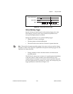
Note
If you are using a version of NI-DAQ prior to version 6.8, the minimum value for
the interval parameter is 2.