


Chapter 4 Signal Connections
©
National Instruments Corporation 4-3 PCI-6110E/6111E User Manual
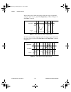
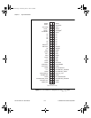
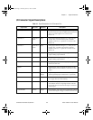
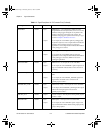
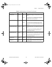
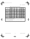
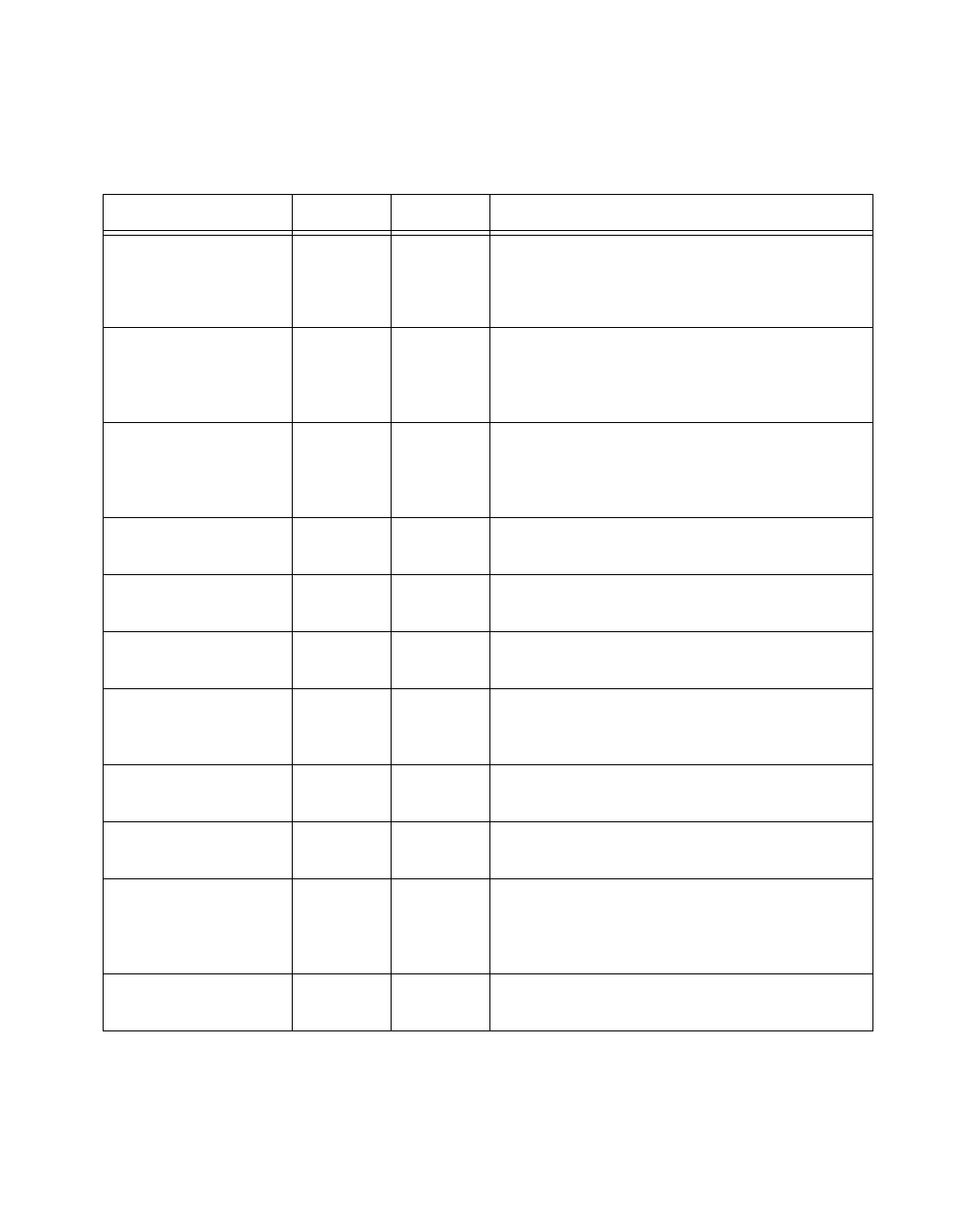
I/O Connector Signal Descriptions
Table 4-1.
Signal Descriptions for I/O Connector Pins
Signal Name Reference Direction Description
ACH <0..3> GND — — Analog Input Channels 0 through 3 ground—These pins are
the bias current return point for differential measurements.
ACH <2..3> GND signals are no connects on the
PCI-6111E.
ACH<0..3> + ACH <0..3>
GND
Input Analog Input Channels 0 through 3 (+)—These pins are
routed to the (+) terminal of the respective channel’s
amplifier. ACH <2..3> + signals are no connects on the
PCI-6111E.
ACH<0..3> – ACH <0..3>
GND
Input Analog Input Channels 0 through 3 (–)—These pins are
routed to the (–) terminal of the respective channel’s
amplifier. ACH <2..3> – signals are no connects on the
PCI-6111E.
DAC0OUT AOGND Output Analog Channel 0 Output—This pin supplies the voltage
output of analog output channel 0.
DAC1OUT AOGND Output Analog Channel 1 Output—This pin supplies the voltage
output of analog output channel 1.
AOGND — — Analog Output Ground—The analog output voltages are
referenced to this node.
DGND — — Digital Ground—This pin supplies the reference for the
digital signals at the I/O connector as well as the +5 VDC
supply.
DIO<0..7> DGND Input or
Output
Digital I/O signals—DIO6 and 7 can control the up/down
signal of general-purpose counters 0 and 1, respectively.
+5 V DGND Output +5 VDC Source—These pins are fused for up to 1 A of
+5 V supply. The fuse is self-resetting.
SCANCLK DGND Output Scan Clock—This pin pulses once for each A/D conversion
when enabled. The low-to-high edge indicates when the
input signal can be removed from the input or switched to
another signal.
EXTSTROBE* DGND Output External Strobe—This output can be toggled under software
control to latch signals or trigger events on external devices.
PCI_E.book Page 3 Thursday, June 25, 1998 12:55 PM