


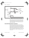
Chapter 4 Signal Connections
PCI-6110E/6111E User Manual 4-20
©
National Instruments Corporation
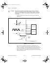
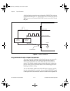
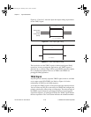
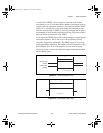
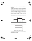
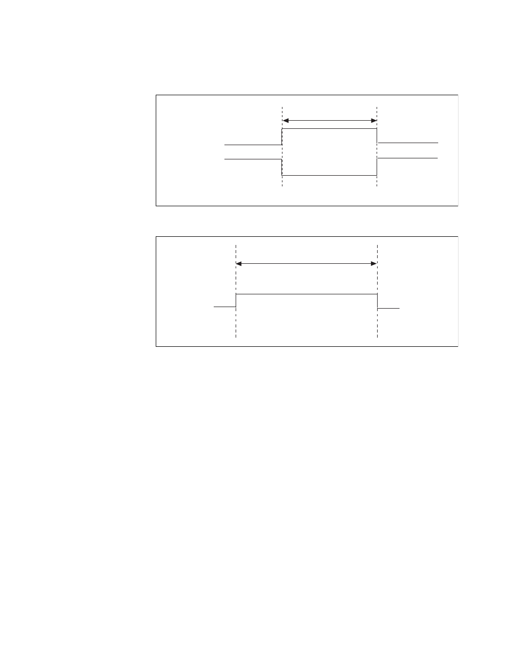
Figures 4-12 and 4-13
show the input and output timing requirements
for the TRIG1 signal.
Figure 4-12. TRIG1 Input Signal Timing
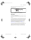
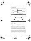
Figure 4-13. TRIG1 Output Signal Timing
The board also uses the TRIG1 signal to initiate pretriggered DAQ
operations. In most pretriggered applications, the TRIG1 signal is
generated by a software trigger. Refer to the TRIG2 signal description
for a complete description of the use of TRIG1 and TRIG2 in a
pretriggered DAQ operation.
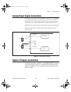
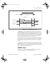
TRIG2 Signal
Any PFI pin can externally input the TRIG2 signal, which is available
as an output on the PFI1/TRIG2 pin. Refer to Figure 4-9 for the
relationship of TRIG2 to the DAQ sequence.
As an input, the TRIG2 signal is configured in the edge-detection mode.
You can select any PFI pin as the source for TRIG2 and configure the
polarity selection for either rising or falling edge. The selected edge of
the TRIG2 signal initiates the posttriggered phase of a pretriggered
acquisition sequence. In pretriggered mode, the TRIG1 signal initiates
the data acquisition. The scan counter indicates the minimum number
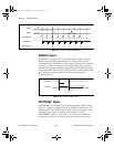
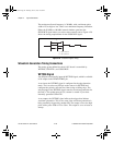
Rising-edge
polarity
Falling-edge
polarity
t
w
t
w
= 10 ns minimum
t
w
t
w
= 25-50 ns
PCI_E.book Page 20 Thursday, June 25, 1998 12:55 PM