


Chapter 4 Signal Connections
PCI-6110E/6111E User Manual 4-8
©
National Instruments Corporation
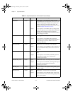
Analog Input Signal Connections
The analog input signals for the 611
X
E board are ACH<0..3>+ and
ACH<0..3>–. The ACH<0..3>+ signals are routed to the positive input
of the PGIA, and signals connected to ACH<0..3>– are routed to the
negative input of the PGIA.
Caution: Exceeding the differential and common-mode input ranges distorts your
input signals. Exceeding the maximum input voltage rating can damage
the 611X E board and the computer. National Instruments is
NOT
liable for
any damages resulting from such signal connections. The maximum input
voltage ratings are listed in the
Protection
column of Table 4-2.
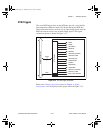
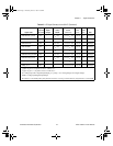
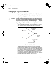
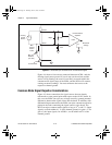
With the different configurations, you can use the PGIA in different
ways. Figure 4-2 shows a diagram of your 611
X
E board PGIA.
Figure 4-2.
611
X
E
Board PGIA
The PGIA applies gain and common-mode voltage rejection and
presents high input impedance to the analog input signals connected to
the 611
X
E board. Signals are routed to the positive and negative inputs
of the PGIA. The PGIA converts two input signals to a signal that is the
difference between the two input signals multiplied by the gain setting
of the amplifier. The amplifier output voltage is referenced to the
ground for the board. The 611
X
E board A/D converter (ADC) measures
this output voltage when it performs A/D conversions.
!
-
Instrumentation
Amplifier
-
Measured
Voltage
V
m
+
+
PGIA
V
in+
V
in-
V
m
= [V
in+
- V
in-
]* Gain
PCI_E.book Page 8 Thursday, June 25, 1998 12:55 PM