


Chapter 4 Signal Connections
PCI-6110E/6111E User Manual 4-34
©
National Instruments Corporation
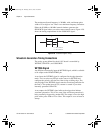
GPCTR1_UP_DOWN Signal
This signal can be externally input on the DIO7 pin and is not available
as an output on the I/O connector. General-purpose counter 1 counts
down when this pin is at a logic low and counts up at a logic high.
This input can be disabled so that software can control the up-down
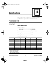
functionality and leave the DIO7 pin free for general use. Figure 4-32
shows the timing requirements for the GATE and SOURCE input
signals and the timing specifications for the 611
X
E board OUT output
signals.
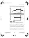
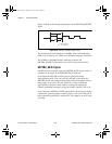
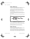
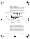
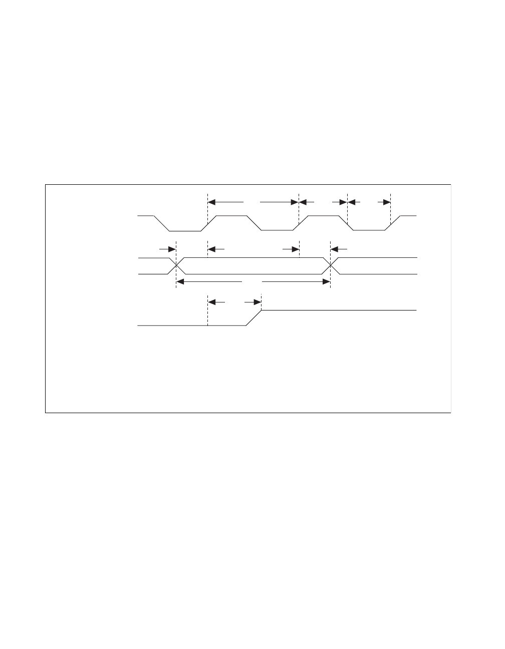
Figure 4-32.
GPCTR Timing Summary
The GATE and OUT signal transitions shown in Figure 4-32 are
referenced to the rising edge of the SOURCE signal. This timing
diagram assumes that the counters are programmed to count rising
edges. The same timing diagram, but with the source signal inverted
and referenced to the falling edge of the source signal, would apply
when the counter is programmed to count falling edges.
The GATE input timing parameters are referenced to the signal at the
SOURCE input or to one of the internally generated signals on the
611
X
E board. Figure 4-32 shows the GATE signal referenced to the
rising edge of a source signal. The gate must be valid (either high or
SOURCE
V
IH
V
IL
V
IH
V
IL
t
sc
t
sp
t
gsu
t
gh
t
gw
GATE
t
out
OUT
V
OH
V
OL
sc
t
t
t
t
t
t 50 ns minimum
sp
23 ns minimum
gsu
10 ns minimum
gh
0 ns minimum
gw
10 ns minimum
out
80 ns maximum
Source Clock Period
Source Pulse Width
Gate Setup Time
Gate Hold Time
Gate Pulse Width
Output Delay Time
t
sp
PCI_E.book Page 34 Thursday, June 25, 1998 12:55 PM