


Chapter 4 Signal Connections
PCI-6110E/6111E User Manual 4-6
©
National Instruments Corporation
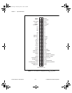
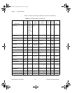
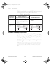
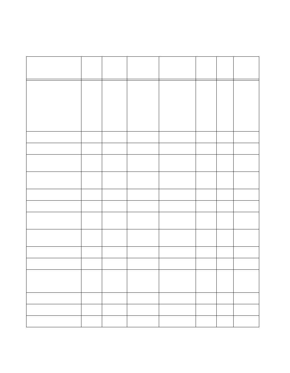
Table 4-2 shows the I/O signal summary for the 611
X
E
boards.
Table 4-2. I/O Signal Summary for the 611
X
E
Signal Name
Signal
Type and
Direction
Impedance
Input/
Output
Protection
(Volts)
On/Off
Source
(mA at V)
Sink
(mA
at V)
Rise
Time
(ns)
Bias
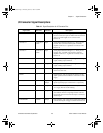
ACH<0..3> + AI 1M
Ω
in parallel
with
100 pF
1
1M
Ω
in parallel
with
10 pF
2
42 V — — — —
ACH<0..3> – AI 10 nF 42 V — — — ±200 pA
ACH <0..3> GND AI — — — — — —
DAC0OUT AO 50
Ω
Short-circuit
to ground
5 at 10 5 at -10 300
V/µs
—
DAC1OUT AO 50
Ω
Short-circuit
to ground
5 at 10 5 at -10 300
V/µs
—
AOGND AO — — — — — —
DGND DO — — — — — —
VCC DO 0.1
Ω
Short-circuit
to ground
1 A — — —
DIO<0..7> DIO — V
cc
+0.5 13 at (V
cc
-0.4) 24 at
0.4
1.1 50 k
Ω
pu
SCANCLK DO — — 3.5 at (V
cc
-0.4) 5 at 0.4 1.5 50 k
Ω
pu
EXTSTROBE* DO — — 3.5 at (V
cc
-0.4) 5 at 0.4 1.5 50 k
Ω
pu
PFI0/TRIG1 AI
DIO
10 k
Ω
±35
V
cc
+0.5
3.5 at (V
cc
-0.4) 5 at 0.4 1.5 9k
Ω
pu
and 10 k
Ω
pd
PFI1/TRIG2 DIO — V
cc
+0.5 3.5 at (V
cc
-0.4) 5 at 0.4 1.5 50 k
Ω
pu
PFI2/CONVERT* DIO — V
cc
+0.5
3.5 at (V
cc
-0.4) 5 at 0.4 1.5 50 k
Ω
pu
PFI3/GPCTR1_SOURCE DIO — V
cc
+0.5 3.5 at (V
cc
-0.4) 5 at 0.4 1.5 50 k
Ω
pu
PCI_E.book Page 6 Thursday, June 25, 1998 12:55 PM