


Chapter 4 Signal Connections
PCI-6110E/6111E User Manual 4-28
©
National Instruments Corporation
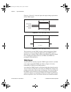
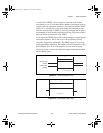
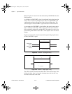
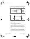
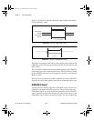
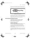
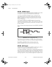
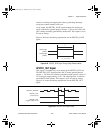
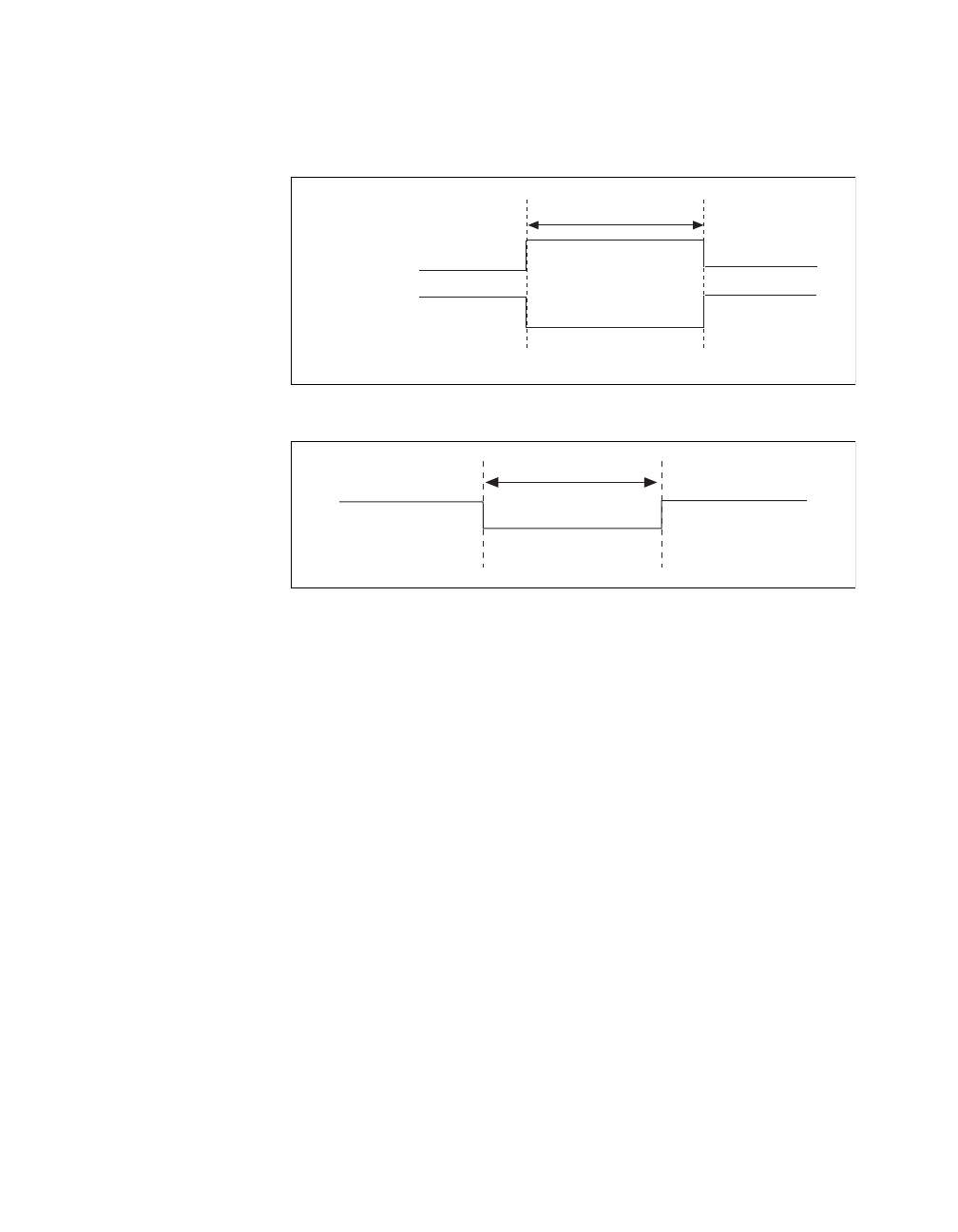
Figures 4-23 and 4-24
show the input and output timing requirements
for the UPDATE* signal.
Figure 4-23. UPDATE* Input Signal Timing
Figure 4-24. UPDATE* Output Signal Timing
The DACs are updated within 100 ns of the leading edge. Separate the
UPDATE* pulses with enough time that new data can be written to the
DAC latches.
The UI counter for the 611
X
E board normally generates the UPDATE*
signal unless you select some external source. The UI counter is started
by the WFTRIG signal and can be stopped by software or the internal
Buffer Counter.
D/A conversions generated by either an internal or external UPDATE*
signal do not occur when gated by the software command register gate.
UISOURCE Signal
Any PFI pin can externally input the UISOURCE signal, which is not
available as an output on the I/O connector. The UI counter uses the
UISOURCE signal as a clock to time the generation of the UPDATE*
signal. You must configure the PFI pin you select as the source for the
UISOURCE signal in the level-detection mode. You can configure the
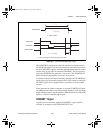
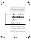
Rising-edge
polarity
Falling-edge
polarity
t
w
t
w
= 10 ns minimum
t
w
t
w
= 50-75 ns
PCI_E.book Page 28 Thursday, June 25, 1998 12:55 PM