SMSC LAN91C111 32/16/8-Bit Three-In-One Fast Ethernet Controller
SMSC AN 9.6 11 Revision 1.0 (08-14-08)
APPLICATION NOTE
3.5.11 32-Bit Access and nBE0-nBE3
The LAN91C111 can operate in 32, 16, or 8-bit mode. Since the registers are assigned to different
banks, changing bank is required if accessing to registers at other bank. Changing bank can be done
by writing to Offset E – Bank Select Register, however offset C, D, E, F are in the same double word
(32-bit) alignment, writing a double word to offset C, will only write to offset E, and will not write to
Offset C, D, and F, because the chip only decodes the bank select register bits. Thus when writing to
Offset C, D, it must be 8 or 16-bit mode. In 8 or 16-bit access, nBE pins have to be asserted
appropriately. For example, if Low word is accessed, nBE[0-1] pins has to be asserted, and nBE[2-3]
must be pulled high.
For read, all registers can be read in 32, 16, or 8-bit mode.
3.5.12 NADS and NCYCLE
nADS (Address Strobe) and nCYCLE indicate that the address is valid to the LAN91C111. The
nCYCLE signal is created externally by delaying the ADS signal by one LCLK cycle. The processor or
bus master must drive valid data on the bus prior to asserting nCYCLE. The nCYCLE pin is discussed
in detail under the nDATACS mode of operations.
The LAN91C111 does not support burst mode operations on the VL-Bus interface in VL-Bus mode.
There is burst type capabilities using nDATACS mode, please see nDATACS mode of operations
described in detail later on in this document.
3.5.13 INTR0
This pin operates as a level-triggered interrupt pin with an active high level. It is typically connected to
IRQ9 but can be connected to whatever interrupt input pin is suitable for your design.
3.5.14 Data Bus
32-bit Data Bus of the LAN91C111. Byte steering is controlled using the BE0-BE3 pins.
3.5.15 NLDEV
nLDEV is used to indicate that the cycle being presented has been claimed by an external device, in
this case the LAN91C111 is claiming the cycle once a valid qualified address decode is accomplished.
The LAN91C111 will assert nLDEV to acknowledge the cycle being presented to it. The timing required
for nLDEV to be asserted is processor specific. Please review the timing requirements for your
particular design. On the LAN91C111 nLDEV is designed to assert in a minimum of 20nS after a valid
address decode. It must be buffered using an open collector driver in ISA bus.
3.6 Timing Analysis
One way to better understand how this interface works is to examine the timing diagrams presented
in the Data Sheet in some details. This is the goal of this section. Below are a timing diagram and the
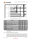
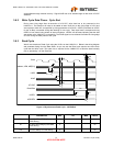
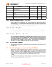
parameter table for a write cycle presented to the LAN91C111 device.


