SMSC LAN91C111 32/16/8-Bit Three-In-One Fast Ethernet Controller
Revision 1.0 (08-14-08) 14 SMSC AN 9.6
APPLICATION NOTE
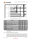
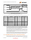
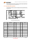
3.6.4 Read Cycle Address Phase – Cycle Start
As with the Write Cycle, the Address Bus, AEN, and the Byte Enable lines (nBE0-nBE3) are required
to be stable 8nS prior to the de-assertion of nADS and 5nS after this rising edge to guarantee a valid
address latching. nLDEV is asserted within 30nS to indicate that the LAN91C111 has claimed this
cycle. The nCYCLE signal will also again need to be generated externally and asserted after address
latching. W/nR should be stable at a low logic level after nCYCLE assertion.
3.6.5 Read Cycle Delay Phase
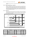
Unlike the Write Cycle, there is a delay required during read operations to allow the LAN91C111 to
fetch the required data. This phase occurs immediately after the address phase and is completed in
one LCLK cycle. During this time the Data Bus is not required to be stable, nor is the address bus.
3.6.6 Read Cycle Data Phase – Cycle End
As the timing diagram represents, the read data is presented from the LAN91C111 on the data bus
and it is guaranteed to be stable at the rising edge when nSRDY (translated to nLRDY for the VL-Bus)
is asserted. nSRDY and data remain stable until the LAN91C111 receives nRDYRTN asserted on the
rising edge of LCLK plus hold time as specified by t20. The nRDYRTN and nSRDY signals indicate
that the LAN91C111 has completed the cycle successfully. W/nR signal should be de-asserted only
after nSRDY is de-asserted, therefore 7nS after LCLK rising with nSRDY active.
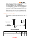
3.6.7 VL-Burst Mode Operation
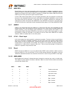
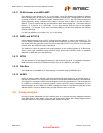
Burst Mode operations as defined by the VESA standard are not supported by the LAN91C111 device
in VL-Bus mode.
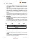
3.7 Direct Data Register Access interface (nDATACS)
Another option available for design engineers to connect to the LAN91C111 is through a direct
interface. This interface is controlled using the nDATACS pin and allows a designer to connect a
controller directly to the LAN91C111 Data Register by bypassing the internal BIU decoders. This
section will discuss in some detail the information necessary to accomplish this interface. This interface
is always
32-bits in nature and therefore the use of the BE0-BE3 pins are ignored.
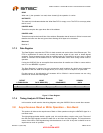
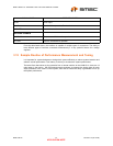
The LAN91C111 offers the design engineer several options as to how this mode of operation can be
implemented. The choices are between synchronous and asynchronous, burst and non-burst modes.
Each of these options will be discussed in detail below.
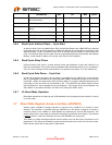
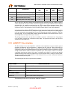
t11 nCYCLE Hold after LCLK Rising
(Non-Burst Mode)
3ns
t16 W/nR Setup to nCYCLE Active 0 ns
t20 Data Hold from LCLK Rising
(Read)
4ns
t21 nSRDY Delay from LCLK Rising 7 ns
t23 nRDYRTN Setup to LCLK Rising 3 ns
t24 nRDYRTN Hold after LCLK Rising 3 ns
PARAMETER MIN TYP MAX UNITS


