


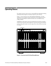


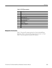

Reference
3–2
VX1410A & VX1420A IntelliFrame Mainframe Instruction Manual
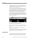
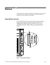
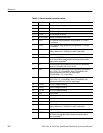
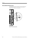
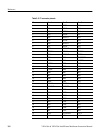
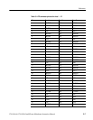
Table 3–1: Passive monitor connector pinouts
Pin Function Description
1 +5 VM +5 V for voltage monitoring
1
2 –12 VM –12 V for voltage monitoring
1
3 –24 VM –24 V for voltage monitoring
1
4 –2 VM –2 V for voltage monitoring
1
5 Rem On/Stdby Remote On/Standby Power Switch.
2
6 +5 VC +5 V output for charging batteries, running external TTL circuitry,
1 A maximum
7 +12 VC +12 V output for charging batteries, running external TTL circuitry,
1 A maximum
8 +5 VB Input for +5 V standby voltage (for example, from an external
battery). Maximum of 1 A total (pins 8 and 21 combined)
3
9 Gnd Logic Ground
10 SYSRESET* Backplane SYSRESET* signal (input or output). If you use this pin,
do not violate VXIbus electrical specifications (keep the extender
cable as short as possible).
4
11 ∆T An analog output signal proportional to the maximum temperature
rise of the 13 modules (100 mV/°C) 0V=0°C
12 Tach1 VX1410A: A square wave output signal proportional to the speed of
Fan 1. RPM = 15 / (+Pulse Width), where (+Pulse Width) is the
positive pulse width of the Tach1 fan output signal.
VX1420A: RPM = 10 / (+Pulse Width)
13 Tach2 VX1410A: A square wave output signal proportional to the speed of
Fan 2. RPM = 15 / (+Pulse Width), where (+Pulse Width) is the
positive pulse width of the Tach2 fan output signal.
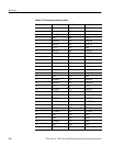
14 +12 VM +12 V for voltage monitoring
1
15 +24 VM +24 V for voltage monitoring
1
16 –5.2 VM –5.2 V for voltage monitoring
1
17 Gnd Logic Ground
18 Gnd Logic Ground
19 Gnd Logic Ground
20 Gnd Logic Ground
21 +5 VB Input for +5 V standby voltage (for example, from an external
battery). Maximum of 1 A total (pins 8 and 21 combined)
3
22 Gnd Logic Ground
23 ACFAIL* Backplane ACFAIL* signal output. If you use this pin, do not violate
the VXIbus electrical specifications (keep the extender cable as
short as possible).
4