


EPSON Stylus PHOTO 810/820/830 Revision B
Operating Principles Electrical Circuit Operating Principles 50
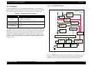
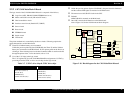
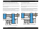
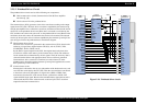
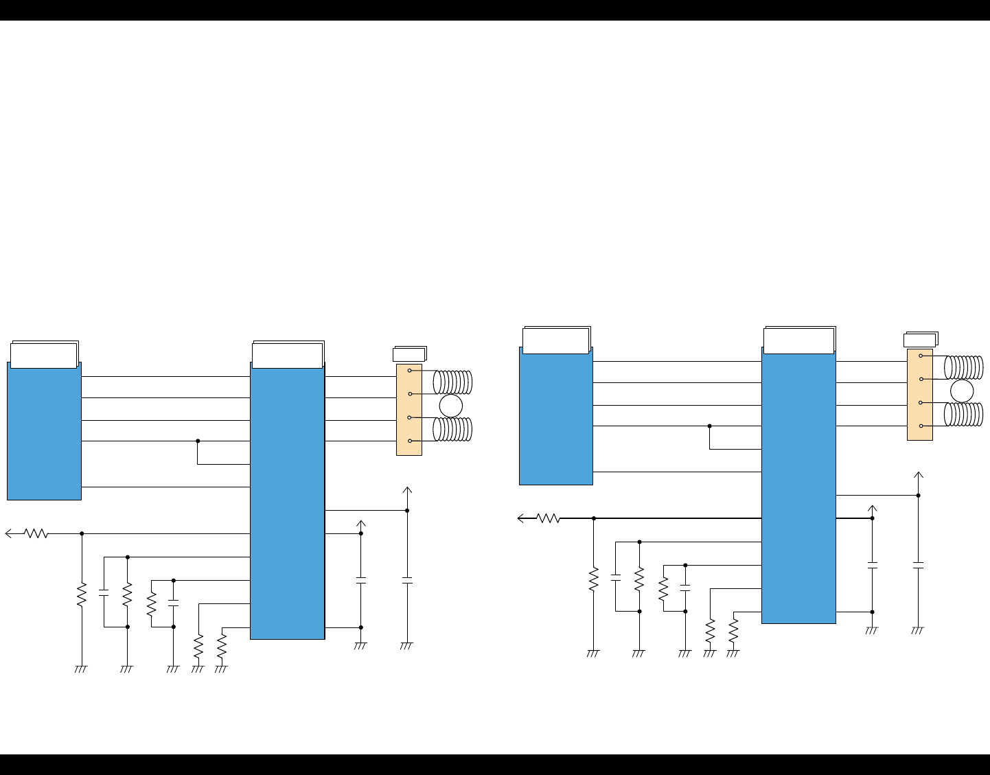
2.2.2.3 PF Motor (PF/ PUMP/ ASF Motor) Driver Circuit
The motor driver IC (IC10) on the Main board drives PF motor. This product uses 4-
phase 96-poles hybrid type stepping motor and performs constant current bi-polar
drive.
CPU (IC1) transmits LB1946 micro step drive form and the current value data on each
phase to motor driver IC (IC10) from port 139. Based on this signal, motor driver IC
determines the phase mode.
Motor driver IC generates motor driver waveform based on these input signals and
controls the motor. And also, motor driver IC monitors to prevent the fluctuations in
the actual current value to motor driver IC. If motor driver IC detects the fluctuations in
the actual current value, it amends the current value internally.
In case that the printer dose not receive any data for 5 minutes, CPU set the motor drive
current to 0 [A] and the motor drive is turned off to save the power consumption.
Figure 2-20. PF motor driver circuit block diagram
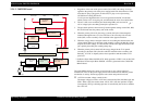
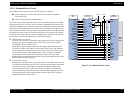
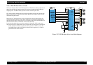
2.2.2.4 CR Motor Driver Circuit
The motor driver IC (IC11) on the Main board drives CR motor. This product uses 4-
phase 200-poles hybrid type stepping motor and performs constant current bi-polar
drive.
CPU (IC1) transmits LB1946 micro step drive form and the current value date on each
phase to motor driver IC (IC11) from port 142. Based on this signal, motor driver IC
determines the phase mode.
Motor driver IC generates motor driver waveform based on these input signals and
controls the motor. And also, motor driver IC monitors to prevent the fluctuations in
the actual current value to motor driver IC. If motor driver IC detects the fluctuations in
the actual current value, it amends the current value internally.
In case that the printer dose not receive any data for 5 minutes, CPU set the motor drive
current to 0 [A] and the motor drive is turned off to save the power consumption.
Figure 2-21. CR motor driver circuit block diagram
CPU
(IC1)
CLK
DATA
SET
VREF1
VREF2
ST
LB1946
(IC10)
CN7
+42v
+5V
+5V
MD
CR1
CR2
E1
E2
OUTA
OUTA-
OUTB
OUTB-
VBB
VCC
PF-SCLK
PF-DATA
PF-LAT
C-P47
C-P25
138
139
140
3
144
23
22
21
27
16
20
24
25
18
3
12
7
6
9
8
1
28
1
3
2
4
CPU
(IC1)
CLK
DATA
SET
VREF1
VREF2
ST
LB1946
(IC11)
CN12
+42v
+5V
+5V
MD
CR1
CR2
E1
E2
OUTA
OUTA-
OUTB
OUTB-
VBB
VCC
CR-SCLK
CR-DATA
CR-LAT
C-P46
C-P25
141
142
143
4
144
23
22
21
27
16
20
24
25
18
3
12
7
6
9
8
1
28
1
3
2
4