


Intel NetStructure
®
MPCBL0001 High Performance Single Board Computer 23
Technical Product Specification
Features Overview
— DMA channels (transmit, receive, command, auto-request, and auto-response)
• Support for JTAG boundary scan.
• Supports IP as well as other protocols; however there are currently no plans to validate
protocols other than SCSI_FCP.
Each Fibre Channel interface of the ISP2312 includes its own internal 16-bit RISC processor and
external 7.5 ns synchronous SRAM memory for instruction code and data. Parity protection is
provided on accesses to this memory. The SBC utilizes two 256 KByte (128Kx18) SRAMs, one for
each port, for the ISP2312 memory requirements.
An external 256 x 16 non-volatile EEPROM is used to store system configuration parameters and
PCI subsystem and subsystem vendor IDs. The first 128 bytes are used for function 0 parameters
and the second 128 bytes are used for function 1.
2.2.5 PMC Connector (J25, J26, J27)
The MPCBL0001 SBC supports one 64-bit, 66 MHz PMC slot. The PMC slot is connected to the
second of two P64H2 hub controllers via PMC Connectors J25-J27. The PMC slot has an opening
in the front panel of the SBC that exposes the I/O connectors of the add-in PMC card. PMC cards
can only be added to or removed from this slot when the board is outside the system chassis. See
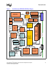
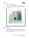
Figure 20, “Intel NetStructure® MPCBL0001 Component Layout” on page 90 for its location.
The PCI bus specification provides the means for backward compatibility with slower PMC cards
(32-bit or 33 MHz) through the use of the M66EN pin. A PMC card that does not support 66 MHz
operation grounds the M66EN pin when installed to inform the SBC hardware to provide a 33
MHz clock to this interface. Support for 32-bit only PMC cards is accomplished through the use of
the REQ64#/ACK64# PCI bus protocol.
The PMC slot provided by the SBC connects the PCI VI/O voltage pins to +3.3 V. This requires
use of PMC plug-in cards that support +3.3 V I/O signal levels. Only PMC plug-in cards
designated “+3.3 V only” or “universal” voltage I/O are supported. The PMC plug-in location
provides a key pin to prevent insertion of cards that do not meet this requirement. Note that +5 V
power is still supplied to the PMC pins designated for +5 V connections. The PMC is allotted 1.5 A
of current.
2.2.6 Firmware Hub (U30, U33)
The MPCBL0001 SBC supports two 8Mbit (1 MByte) BIOS flash ROMs:
• Primary BIOS flash ROM (FWH0)
• Recovery BIOS flash ROM (FWH1)
The flash is allocated for BIOS and Firmware usage.
The SBC boots from the primary flash ROM under normal circumstances. During the boot process,
if the BIOS (or IPMC) determines that the contents of the primary flash ROM are corrupted, a
hardware mechanism is available to change the flash device select logic to the recovery flash
ROM. See Section 2.2.6.3, “Flash ROM Backup Mechanism” on page 24 for more information.
Each flash component has a separately write-protected boot block that prevents erasure when the
device is upgraded.