


60 Intel NetStructure
®
MPCBL0001 High Performance Single Board Computer
Technical Product Specification
Hardware Management Overview
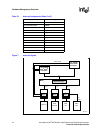
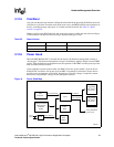
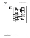
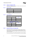
As the many voltages power up, each regulator produces a “power good” signal. All of these power
good signals are logically OR’d (with the exception of the VRM power good) to produce the
ICH3_PWROK signal input to the ICH3 as shown in Figure 8, Power Good Map. When this signal
is active, it indicates all on-board power is good.
Next, the VRM power good is gated with the ICH3_PWROK signal in the ICH3 to produce the
processor’s power good signal input.
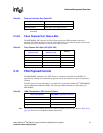
As soon as the ICH3 device is powered, its PCI reset output is asserted. This reset output remains
asserted until all power good signals are present (indicated by the ICH3_PWROK signal), the
processor VRM power good signal is asserted, and device voltage/clock stabilization times have
been satisfied.
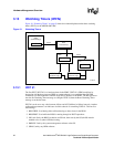
Device resets are then released, and processor BIOS execution and boot begins. The PCI reset
output of the ICH3 is the source of all other power-up reset signals as shown in Figure 9, “Reset
Chain” on page 61
The IPMC is also capable of initiating this power-up or global reset by negating the
ICH3_PWROK signal. Additionally, devices on specific PCI buses may be independently reset by
software through their associated bridge devices.
When commanded to do so, the IPMC releases device and processor resets, and processor BIOS
execution and boot begins.