OCPRF100 MP Server System Technical Product Specification
Revision 1.0
99
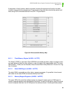
A description of each memory block is provided, showing the purpose and function as deter-
mined by microcontroller programming. These functions may also be controlled by system soft-
ware using SCSI commands defined in the SAF-TE specification.
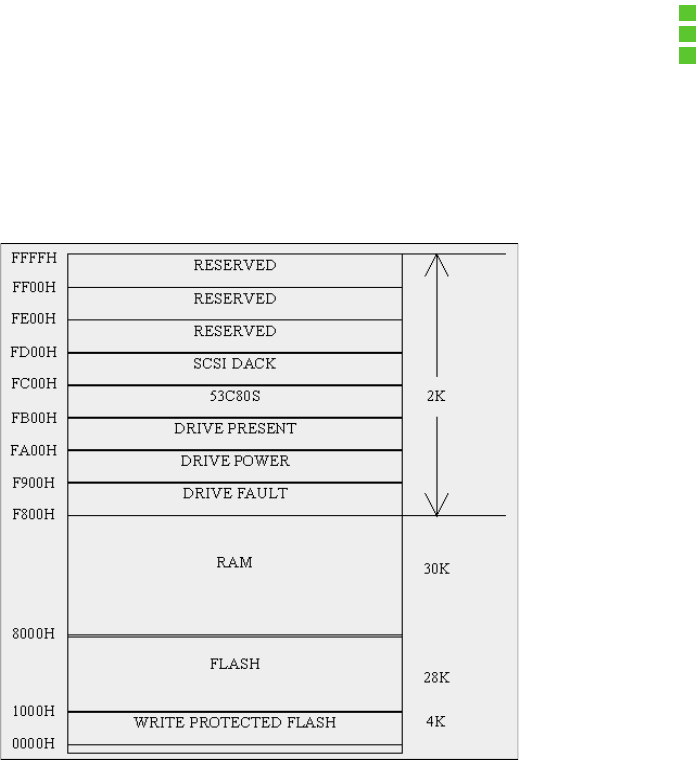
Figure 8-4: Microcontroller Memory Map
8.6.1.1 Flash Memory Region (0x0000 – 0x7FFF)
The Atmel* 27C257 or equivalent Flash EPROM is accessible as either a data or program mem-
ory read. Writes to Flash are also allowed in order to support field-upgradeable code. The lower
4KB (0x0000 – 0x0fff) are not writeable unless the boot block write protect bit in the fan mux reg-
ister is cleared.
8.6.1.2 Static RAM Region (0x8000 – 0xF7FF)
The static RAM is accessible as either data or program accesses. It is possible to load execut-
able code into the static RAM and execute directly from RAM.
8.6.1.3 Memory Mapped Registers (0xF800 – 0xFFFF)
The upper 2KB of the controller address space are mapped to eight regions of 256 bytes for
memory-mapped registers and miscellaneous functions. For each of the regions listed, the actual
function occupies less than the full 256 bytes of its address decode. Unless specifically stated,


