OCPRF100 MP Server System Technical Product Specification
Revision 1.0
115
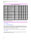
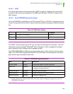
10.2.2.1 Device Maps
10.2.2.2 I/O Memory Maps
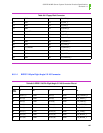
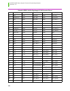
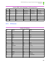
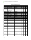
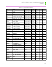
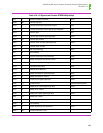
Table 10-2: I/O Signals and Devices provides a cross reference between the I/O signals and the
individual devices. These can be referenced against the device map section to resolve the abso-
lute address.
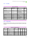
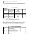
Table 10-1: Device Maps
Function Address Range Access Width
Output Latch #1 FFF0 - FFFF Write
(Read RAM Shadow)
Byte
Output Latch #0 FFE0 - FFEF Write
(Read RAM Shadow)
Byte
RAM, Output Latch Shadow FF00 - FFFF Execute, Read, Write
(Shadows Output Latches)
Byte
Input Latch #1 FFD0 - FFDF Read Byte
Input Latch #0 FFC0 - FFCF Read Byte
PLD FE00 - FFFF Read, Write Byte
RAM # 0 E000 - FDFF Execute, Read, Write Byte
FLASH, OPS 1000 - DFFF Execute, Read, Write Byte
FLASH, BOOT 0000 - 0FFF Execute, Read Byte
Table 10-2: I/O Signals and Devices
Topic Signal Device Addres
s
Acces
s
Offset Bit
Not Applicable Not Applicable
(Muxed Address/Data BUS)
Micro Port 0 - - - 0 to 7
LCD LCD_RW Micro Port 1 - RW - 0
LCD LCD_EN Micro Port 1 - RW - 1
LCD LCD_RS Micro Port 1 - RW - 2
Miscellaneous RESET_OUTPUTS_L Micro Port 1 - RW - 3


