


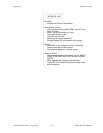
Sample Programs Appendix C
GPIB-1014 User Manual C-2 © National Instruments Corporation
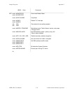
;;;;;;;;;;;;;;;;;;;;;;;;;;;;;;;;;;;;;;;;;;;;;;;;;;;;;;;;;;;;;;;;;;;;;;;
|;
| GPIB-1014 Sample Functions for Driver: ;
|;
| INIT (Initialize the GPIB-1014) ;
| IFC (Send Interface Clear) ;
| REN (Set/Clear Remote Enable) ;
| RCV (Receive) ;
| READ (Read Data) ;
| DSEND (Data Send) ;
| WRITE (Write Data) ;
| CSEND (Command Send) ;
| CMD (Write Commands) ;
| PASSC (Pass Control) ;
|;
;;;;;;;;;;;;;;;;;;;;;;;;;;;;;;;;;;;;;;;;;;;;;;;;;;;;;;;;;;;;;;;;;;;;;;;;;;;;;;;;;;;;;
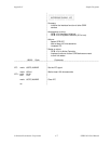
|
|
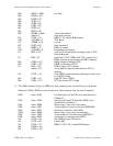
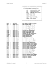
BASE = 0xFF2000 | Base address of GPIB-1014 interface
DIR = BASE + 0x111 | Data In Register (read)
CDOR = BASE + 0x111 | Control/Data Out Register (write)
ISR1 = BASE + 0x113 | Interrupt Status Register 1 (read)
IMR1 = BASE + 0x113 | Interrupt Mask Register 1 (write)
ISR2 = BASE + 0x115 | Interrupt Status Register 2 (read)
IMR2 = BASE + 0x115 | Interrupt Mask Register 2 (write)
SPSR = BASE + 0x117 | Serial Poll Status Register (read)
SPMR = BASE + 0x117 | Serial Poll Mask Register (write)
ADSR = BASE + 0x119 | Address Status Register (read)
ADMR = BASE + 0x119 | Address Mode Register (write)
CPTR = BASE + 0x11B | Command Pass Thru Register (read)
AUXMR = BASE + 0x11B | Auxiliary Mode Register (write)
ADR0 = BASE + 0x11D | Address Register 0 (read)
ADR = BASE + 0x11D | Address Register (write)
ADR1 = BASE + 0x11F | Address Register 1 (read)
EOSR = BASE + 0x11F | End Of String Register (write)
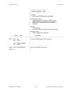
MTC0 = BASE + 0x00A | Channel 0 Memory Transfer Count
MAR0 = BASE + 0x00C | Channel 0 Memory Address Register
MFC0 = BASE + 0x029 | Channel 0 Memory Function Code
CSR0 = BASE + 0x000 | Channel 0 Status Register
DCR0 = BASE + 0x004 | Channel 0 Device Control Register
OCR0 = BASE + 0x005 | Channel 0 Operation Control Register
SCR0 = BASE + 0x006 | Channel 0 Sequence Control Register
CCR0 = BASE + 0x007 | Channel 0 Channel Control Register
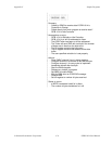
MTC1 = BASE + 0x04A | Channel 1 Memory Transfer Count
MAR1 = BASE + 0x04C | Channel 1 Memory Address Register
MFC1 = BASE + 0x069 | Channel 1 Memory Function Code
BTC1 = BASE + 0x05A | Channel 1 Base Transfer Count
BAR1 = BASE + 0x05C | Channel 1 Base Address Register
BFC1 = BASE + 0x079 | Channel 1 Base Function Code
CSR1 = BASE + 0x040 | Channel 1 Status Register
DCR1 = BASE + 0x044 | Channel 1 Device Control Register
OCR1 = BASE + 0x045 | Channel 1 Operation Control Register
SCR1 = BASE + 0x046 | Channel 1 Sequence Control Register
CCR1 = BASE + 0x047 | Channel 1 Channel Control Register
CFG1 = BASE + 0x101 | Configuration Register 1
CFG2 = BASE + 0x105 | Configuration Register 2