


Chapter 3 Hardware Overview
National Instruments Corporation 3-15 AT-MIO/AI E Series User Manual
Selecting a bipolar range for a particular DAC means that any data
written to that DAC will be interpreted as two’s complement
format. In two’s complement mode, data values written to the
analog output channel can be either positive or negative. If you
select unipolar range, data is interpreted in straight binary format.
In straight binary mode, data values written to the analog output
channel range must be positive.
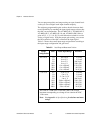
♦ AT-MIO-16XE-10
You can configure each analog output channel for either unipolar
or bipolar output. A unipolar configuration has a range of 0 to 10 V
at the analog output. A bipolar configuration has a range of
-10 to +10 V at the analog output. You do not need to configure
both channels for the same range.
Analog Output Reglitch Selection
♦ AT-MIO-16E-1, AT-MIO-16E-2, and AT-MIO-64E-3 only
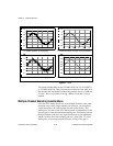
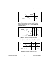
In normal operation, a DAC output will glitch whenever it is
updated with a new value. The glitch energy differs from code to
code and appears as distortion in the frequency spectrum. Each
analog output of the AT-MIO-16E-1, AT-MIO-16E-2, and
AT-MIO-64E-3 contains a reglitch circuit that generates uniform
glitch energy at every code rather than large glitches at the major
code transitions. This uniform glitch energy appears as a multiple
of the update rate in the frequency spectrum. Notice that this
reglitch circuit does not eliminate the glitches; it only makes them
more uniform in size. Reglitching is normally disabled at startup
and can be independently enabled for each channel through
software.
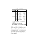
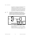
Analog Trigger
♦ AT-MIO-16E-1, AT-MIO-16E-2, AT-MIO-64E-3,
AT-MIO-16XE-10, and AT-AI-16XE-10 only
In addition to supporting internal software triggering and external
digital triggering to initiate a data acquisition sequence, the
AT-MIO-16E-1, AT-MIO-16E-2, AT-MIO-64E-3,
AT-MIO-16XE-10, and AT-AI-16XE-10 also support analog
triggering. You can configure the analog trigger circuitry to accept
either a direct analog input from the PFI0/TRIG1 pin on the I/O
connector or a postgain signal from the output of the PGIA, as