339
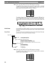
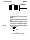
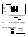
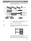
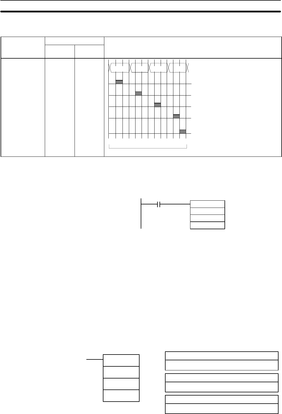
Timing The timing of data output is shown in the following table. “O” is the first word hold-
ing display data and “C” is the output word.
Function
Bit(s) in O
Output status (Data and latch logic depends on C)
(4 digits,
1 block)
(4 digits,
2 blocks)
Latch output 2
Latch output 3
One Round Flag
Latch output 1
Latch output 0
Data output
06
07
08
05
04
00 to 03
10
11
12
09
08
00 to 03
04 to 07
10
0
10
1
10
2
10
3
0123456789101112
Note 0 to 3: Data output for word S
4 to 7: Data output for word S+1
12 cycles required to complete one round
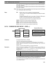
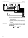
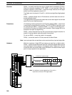
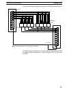
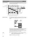
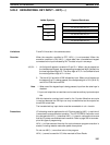
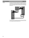
Application Example This example shows a program for displaying 8-digit BCD numbers at a 7-seg-
ment LED display. Assume that the 7-segment display is connected to output
word IR 100. Also assume that the Output Unit is using negative logic, and that
the 7-segment display logic is also negative for data signals and latch signals.
7SEG(––)
DM0120
100
004
25313 (Always ON)
The 8-digit BCD data in DM 0120 (rightmost 4 digits) and DM 0121 (leftmost 4
digits) are always displayed by means of 7SEG(––). When the contents of
DM 0120 and DM 0121 change, the display will also change.
Flags ER: S and S+1 are not in the same data area. (When set to display 8-digit
data.)
Indirectly addressed DM word is non-existent. (Content of DM word is
not BCD, or the DM area boundary has been exceeded.)
There is an error in operand settings.
25409: SR 25409 will be ON while 7SEG(––) is being executed.
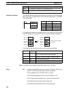
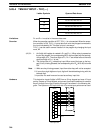
5-28-2 DIGITAL SWITCH INPUT – DSW(––)
IW: Input word
IR, SR, AR, DM, HR, LR
Ladder Symbols Operand Data Areas
DSW(––)
IW
OW
R
R: First result word
IR, SR, AR, DM, HR, LR
OW: Output word
IR, SR, AR, DM, HR, LR
Advanced I/O Instructions Section 5-28


