


Warranted Characteristics
1–18
TDS 684A, TDS 744A, & TDS 784A Service Manual
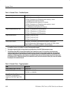
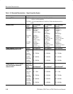
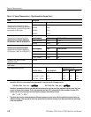
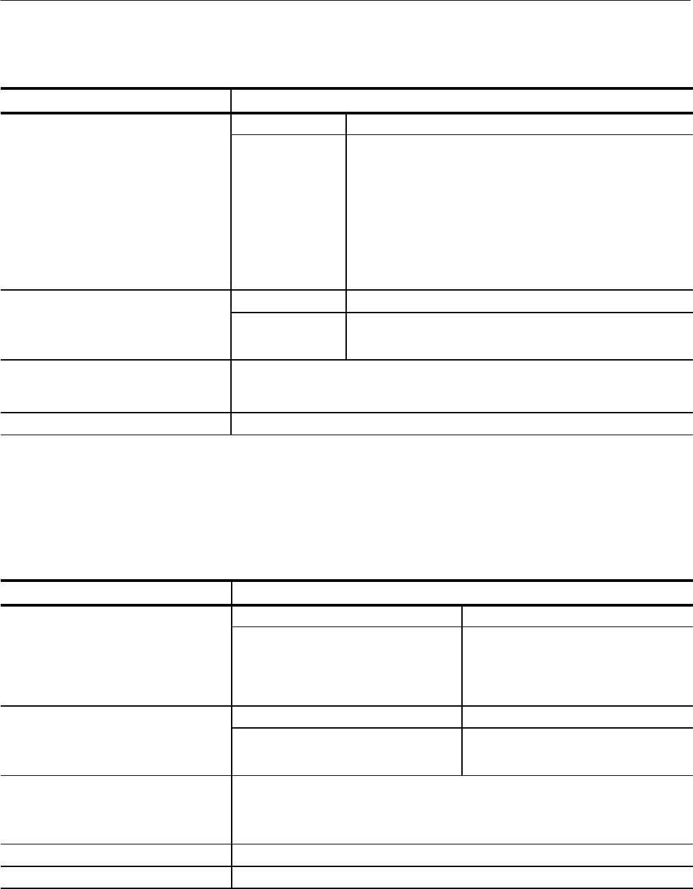
Table 1–12: Warranted Characteristics — Triggering System
Name Description
Sensitivity, Edge-Type Trigger, Coupling
set to “DC”
1
Trigger Source Sensitivity
Sensitivity, Edge-Type Trigger, Coupling
set to “DC”
1
Any Channel
Auxiliary
TDS 684A: 0.35 division from DC to 50 MHz, increasing to
1 division at 1 GHz
TDS 7XXA: 0.35 division from DC to 50 MHz, increasing to
1 division at 500 MHz for the TDS 744A or to 1 division at 1 GHz
for the TDS 784A
TDS 684A or 784A: 250 mV from DC to 50 MHz, increasing to
500 mV at 100 Mhz
TDS 744A: 400 mV from DC to 50 MHz, increasing to 750 mV at
100 Mhz
Accuracy (Time) for Pulse-Glitch or
Pulse-Width Triggering
Time Range Accuracy
Accuracy (Time) for Pulse-Glitch or
Pulse-Width Triggering
1 ns to 1 ms
1.02 ms to 1 s
±(20% of setting + 0.5 ns)
±(100 ns + 0.01% of Setting)
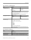
Input Signal Sync Amplitude for Stable
Triggering, NTSC and PAL modes
(Option 05 Video Trigger)
Field selection “Odd”, “Even”, or “All”: 0.6 division to 4 divisions
Field selection “Numeric”: 1 division to 4 divisions (NTSC mode)
Jitter (Option 05 Video Trigger) 60 ns
p-p
on NTSC or PAL signal
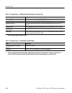
1
The minimum sensitivity for obtaining a stable trigger. A stable trigger results in a uniform, regular display triggered on
the selected slope. The trigger point must not switch between opposite slopes on the waveform, and the display must not
“roll” across the screen on successive acquisitions. The TRIG’D LED stays constantly lighted when the SEC/DIV setting
is 2 ms or faster but may flash when the SEC/DIV setting is 10 ms or slower.
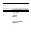
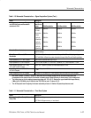
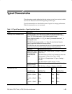
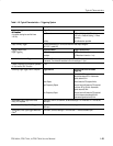
Table 1–13: Warranted Characteristics — Output Ports, Probe Compensator, and Power Requirements
Name Description
Logic Levels, Main- and Delayed-Trigger
Outputs
Characteristic Limits
Logic Levels, Main- and Delayed-Trigger
Outputs
Vout (HI)
Vout (LO)
≥2.5 V open circuit; ≥1.0 V into a 50 W
load to ground
≤0.7 V into a load of ≤4 mA;
≤0.25 V into a 50 W load to ground
Output Voltage and Frequency,
Probe Compensator
Characteristic Limits
Output Voltage and Frequency,
Probe Compensator
Output Voltage
Frequency
0.5 V (base-top) ±1% into a ≥50 W load
1 kHz ±5%
Output Voltage, Signal Out (CH 3
1
) For TDS 684A: 20 mV/division ±20% into a 1 MW load;
10 mV/division ±20% into a 50 W load
For TDS 7XXA: 22 mV/division ±20% into a 1 MW load;
11 mV/division ±20% into a 50 W load
Source Voltage 90 to 250 VAC
RMS
, continuous range
Source Frequency 45 Hz to 440 Hz