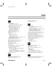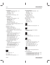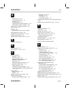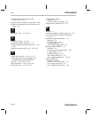
Index
PRELIMINARY
Index-4
PRELIMINARY
subroutines used by all algorithms (SU-
TILS2x.ASM) A-25
SUTILS2x.ASM file (code for subroutines) A-25
SVAR2x.H file (header file for constants and vari-
ables) A-2
T
test register (TST) 2-6, 2-8, 2-10
U
uniformity of charge 3-5, 3-9
unintentional erasure, protection 2-16
using the algorithms with assembly code A-32,
A-40
using the algorithms with C code A-37, A-47
V
variable CPU clock rate 3-5, 3-12, 3-17
variable declaration file.
See
header file for
constants and variables (SVAR2x.H)
VCCP pin 2-16, 3-8, 3-11, 3-15
VER0 read mode 2-12, 2-13, 3-8, 3-9
VER1 read mode 2-12, 2-15, 3-11
verify bits (VER1, VER0)
described 2-9
location in SEG_CTR register 2-8
voltage level for standard read 2-12
W
web page iii
worst–case voltage for reading erased cell 2-12
worst–case voltage for reading programmed
cell 2-12
write address register (WADRS) 2-10
described 2-8
in mode selection 2-6
in program operation 2-13
role in single program pulse 3-8
write data register (WDATA) 2-11
described 2-8
in mechanism for array protection 2-16
in mode selection 2-6
in program operation 2-13
role in single erase pulse 3-11
role in single program pulse 3-8, 3-9
WRITE/ERASE field
described 2-9, 3-8
location in SEG_CTR register 2-8
role in single erase pulse 3-11
role in single flash–write pulse 3-15


