


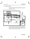


Erase Algorithm
PRELIMINARY
3-12
PRELIMINARY
4) The actual address is restored.
5) The contents of the restored address are read.
The advantage of this approach is that it forces the worst-case switching condi-
tion on the flash addressing logic during the reads, thus improving the margin
of the erase. Address complementing on the ’F20x/F24x can be accomplished
easily by using the XOR instruction to complement the bits of the address.
An important consideration for erasing the flash array is the CPU frequency
range for the application. Because of the actual implementation of the flash
memory circuitry, a logic 1 is most easily read at low frequency; erased bits
have less margin when read at higher frequency. Accordingly, if the application
requires a variable CPU clock rate, the erase should be performed at the high-
est frequency in the range. (A similar condition exists for the programming op-
eration, which requires execution of the programming algorithm at the lowest
frequency in the range. See section 3.2, page 3-4.)
Another important consideration is the total amount of time required to erase
the array. The number of erase pulses required to completely erase a flash
memory cell increases as ambient temperature increases or decreases rela-
tive to the nominal temperature and as supply voltage decreases. More erase
pulses are required when the ambient temperature is toward the extremes of
the operating range. Also, more erase pulses are required when the minimum
supply voltage is used than when the nominal or maximum supply voltage is
used. The number of erase pulses required also increases throughout the life
of the device, as more program-erase cycles are carried out. The device data
sheet specifies the maximum number of erase pulses under all operating con-
ditions; use this number when you calculate the maximum amount of time re-
quired for the erase algorithm.
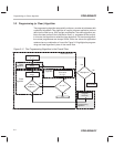
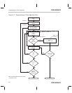
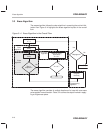
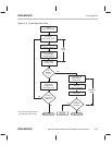
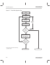
The complete erase algorithm including depletion check is shown in the flow-
chart in Figure 3–5.