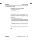
Accessing the Flash Module
PRELIMINARY
2-7
Flash Operations and Control Registers
PRELIMINARY
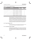
Although the function is the same, the access control registers of the ’F206 de-
vice are mapped at different addresses from that of the ’F24x devices, and
their values are modified in a different way.
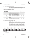
2.2.2 TMS320F24x Flash Access-Control Register
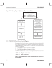
The access-control register of the ’F24x devices is a special type of I/O-
mapped register that cannot be read. The register is mapped at I/O address
0FF0Fh, and it functions as indicated below.
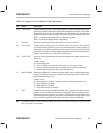
Note:
For both the IN and OUT instructions, the data operand (dummy) is not used,
and can be any valid memory location.
An OUT instruction using the register address as an I/O port places the flash
module in register-access mode.
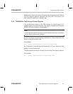
For example:
OUT dummy, 0FF0Fh ;Selects register-access mode
An IN instruction using the register address as an I/O port places the flash
module in array-access mode.
The data operand (dummy) is not used, and can be any valid memory location.
For example:
IN dummy, 0FF0Fh ;Selects array-access mode


