


Accessing the Flash Module
PRELIMINARY
2-6
PRELIMINARY
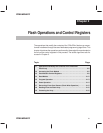
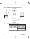
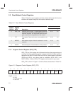
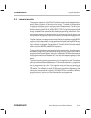
Figure 2–2. Memory Maps in Register and Array Access Modes
SEG_CTR register
TST register
WADRS register
WDATA register
Flash memory
array
Flash access control register
(single bit)
MODE = 1: Array-access mode
MODE = 0: Register access mode
0100 ... 010
0100 ... 011
1110 ...110
0110 ...111
4 registers duplicated
4 registers duplicated
4 registers duplicated
2.2.1 TMS320F206 Flash Access-Control Register
Because each flash module has an access-control register associated with it,
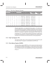
the ’F206 has two access-control registers. These registers are standard I/O-
mapped registers that can be read with an IN instruction and must be modified
with an OUT instruction.
- F_ACCESS0 is mapped in I/O space at 0FFE0h.
- F_ACCESS1 is mapped in I/O space at 0FFE1h.
The MODE bit (bit 0) of the access-control register selects the access mode:
MODE = 0 Register-access mode
MODE = 1 Array-access mode
Bits 15–1 of each access-control register are always read as 0 and are unaf-
fected by writes.