


Reading From the Flash Array
PRELIMINARY
2-16
PRELIMINARY
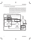
2.8 Reading From the Flash Array
Once the array is programmed, it is read in the same manner as other memory
devices on the DSP memory interface. The flash module operates with zero
wait states. When you are reading the flash module, the flash segment control
register (SEG_CTR) bits should be 0 and the flash array must be in the array-
access mode.
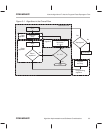
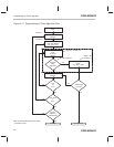
2.9 Protecting the Array
After the flash memory array is programmed, it is desirable to protect the array
against corruption. The flash module of the ’F20x/F24x DSPs includes several
protection mechanisms to prevent unintentional modification of the array.
Flash programming is facilitated via the supply voltage connected to the VCCP
pin. If this pin is grounded, the program operation will not modify the flash array.
Note, that grounding the VCCP pin does not prevent the erase operation; other
protection mechanisms for the erase operation are discussed below.
The control registers provide the following mechanisms for protecting the flash
array from unintentional modification.
- Segment enable bits
- EXE, KEY0, and KEY1 bits
- WDATA register
An array segment is prevented from being programmed when the correspond-
ing segment enable bit in the SEG_CTR is cleared to zero. Additionally, all seg-
ment enable bits are cleared by reset, making unintentional programming less
likely. Even if the segment enable bits are set to one, the program, erase, and
flash-write operations are not initiated unless the appropriate values are set
in the EXE, KEY0, and KEY1 bits of the SEG_CTR.
At the start of an operation, the KEY1 and KEY0 bits must be written in the
same write access that sets EXE. When the program pulse, erase pulse, or
flash-write pulse is finished, EXE must be cleared in the same write that clears
KEY1 and KEY0. The data and address latches are locked whenever the EXE
bit is set, and all attempts to read from or write to the array are ignored (read
data is indeterminate). Once the EXE bit is set, all register bits are latched and
protected. You must clear EXE to modify the SEGx bits. This protects the array
from inadvertent change. Unprotected segments cannot be masked in the
same register load with the deactivation of EXE. Additional security is provided
by a function of the WDATA register to prevent unintentional erasure. The
WDATA register must be loaded with FFFFh before the erase operation is initi-
ated. If the register is not loaded with this value, the array will not be modified.