


Recovering From Over-Erasure (Flash-Write Operation)
PRELIMINARY
2-15
Flash Operations and Control Registers
PRELIMINARY
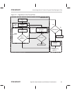
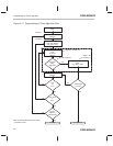
2.7 Recovering From Over-Erasure (Flash-Write Operation)
Generally, not all bits in the flash array have the same amount of charge re-
moved with each erase pulse. By the time all bits have reached the VER1 read
margin (and erase is complete), some of the bits in the array may be over-
erased. They are said to be in depletion mode. If even one single flash cell is
over-erased into depletion mode, it is always read as logic 1 and can corrupt
the reading of other bits. This condition must be detected and corrected, be-
cause it also inhibits reprogramming of the flash array.
The ’F20x/F24x flash array employs the flash-write operation to recover bits
that are erased into depletion mode. The flash-write operation is similar to the
erase operation in that it affects all bits in the array simultaneously. This en-
ables recovery of multiple bits from depletion mode, but requires the flash-
write operation to be followed by the clear and erase operations to restore the
erase margin on all bits.
A
flash-write pulse
is the time during the flash-write operation between the set-
ting and the clearing of the EXE bit (bit 0 of SEG_CTR). During the flash-write
pulse, all array bits are affected simultaneously. (See Figure 2–1,
Flash
Memory Logic Levels During Programming and Erasing
, on page 2-4 for an
illustration of this mechanism.) Multiple flash-write pulses may be required to
fully recover all bits in the array, and the application of flash-write pulses is con-
trolled by the flash-write algorithm.
The flash-write operation uses the inverse-erase read mode and inverse-
erase reference level to detect bits that are in depletion mode. For more infor-
mation about the inverse-erase read mode, see section 2.4,
Read Modes
, on
page 2-12.