Flash Module Control Registers
PRELIMINARY
2-10
PRELIMINARY
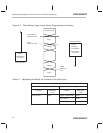
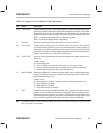
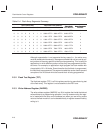
Table 2–4. Flash Array Segments Summary
SEG7–SEG0 Bits ’F206/F240 Flash Module
†
’F241
/
F24
3
Arr
ay
Seg
m
e
nt
15 14 13 12 11 10 9 8 Flash0 Flash1
F241/F243
Flash Module
Array
Segment
Enabled
0
0 0 0 0 0 0 1 0000–07FFh 4000–47FFh 0000–03FFh 0
000000100800–0FFFh 4800–4FFFh 0400–07FFh 1
000001001000–17FFh 5000–57FFh 0800–0BFFh 2
000010001800–1FFFh 5800–5FFFh 0C00–0FFFh 3
000100002000–27FFh 6000–67FFh 1000–13FFh 4
001000002800–2FFFh 6800–6FFFh 1400–17FFh 5
010000003000–37FFh 7000–77FFh 1800–1BFFh 6
1
0 0 0 0 0 0 0 3800–3FFFh 7800–7FFFh 1C00–1FFFh 7
†
The TMS320F206 has two flash modules. The TMS320F240 device uses the address ranges shown for Flash0.
Although segmentation is not supported during erase (i.e., the entire array
must be erased simultaneously), the segment enable bits can be used to pro-
tect portions of the array against unintentional programming. This is useful for
applications in which different portions of the array are programmed at differ-
ent times. For example, an application might program the flash module with
a large table in 2K × 16 blocks. Some time after the first block is programmed,
the next block is programmed. The segment enable bits can be used to prevent
corruption of the first block while the second block is being programmed.
2.3.2 Flash Test Register (TST)
The flash test register (TST) is a 5-bit register used during manufacturing test
of the flash array. This register is not accessible to the DSP core.
2.3.3 Write Address Register (WADRS)
The write address register (WADRS) is a 16-bit register that holds the latched
write address for a programming operation. In array-access mode, this regis-
ter is loaded with the value on the address bus when you are writing a data
value to the flash module. It can be loaded directly in register-access mode by
writing to it.


